<- previous index next ->
Static RAM using 6 transistors per bit. One for set, one for reset,
four in a basic cross coupled nand gate flipflop.

 A mosfet dynamic ram, one transistor and one capacitor.
The capacitor must be refreshed often. RAS mode:
 Mosfet dynamic ram CAS mode:
 Recent generations of DRAM chips contain an integral refresh counter,
and the memory control circuitry can either use this counter or provide
a row address from an external counter. These chips have three standard
ways to provide refresh, selected by different patterns of signals on the
"column select" (CAS) and "row select" (RAS) lines.
"RAS only refresh" - In this mode the address of the row to refresh
is provided by the address bus lines, so it is used with external
counters in the memory controller.
"CAS before RAS refresh" (CBR) - In this mode the on-chip counter keeps
track of the row to be refreshed and the external circuit merely
initiates the refresh cycles. This mode uses less power because the memory
address bus buffers don't have to be powered up. It is used in most modern
computers.
"Hidden refresh" - This is an alternate version of the CBR refresh cycle
which can be combined with a preceding read or write cycle. The refresh
is done in parallel during the data transfer, saving time.
In the latest (2012) generation of chips the "RAS only" mode has been
eliminated, and the internal counter is used to generate refresh.
The chip has an additional "sleep mode", for use when the computer
is in hibernation, in which an on-chip oscillator generates internal
refresh cycles so that the external clock can be shut down.
some review
"Combinational logic" means gates connected together without feedback.
There is no storage of information. Inputs are applied and outputs
are produced. By convention, we draw combinational logic from
inputs on the left to outputs on the right. For large schematic
diagrams this convention is often violated.
When no constraints are given, any of the gates previously
defined can be connected to design a circuit that performs
the stated function.
Example: Design a circuit that has:
an input for tail lights both on
an input for right turn that lets the signal "osc" control right tail light.
an input for left turn that lets the signal "osc" control left tail light.
("osc" will make the light flash on and off as a turn indicator.)
Constraint: use "and" and "or" gates with inversion bubbles allowed
Solution: There are four inputs "tail" "right" "left" and "osc"
There are two outputs "right_light" and "left_light"
The general strategy in design is to work backward from an output.
Yet, as usual, some work from input toward output is also used.
"right_light" must select between "tail" and "osc". Selection
can typically be implemented by "and" gates feeding an "or" gate
with a control signal into one "and" gate and its complement into
the other "and" gate.
 Analyzing this circuit, if "right" is off, "tail" controls
the "right_light". If "right is on, "osc" controls the "right_light".
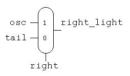
A common symbol for this circuit is a multiplexor, mux for short.
The same circuit as above is usually drawn as the schematic diagram:
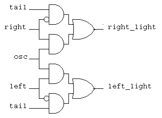
 Now we can use the first schematic with new labeling for
the "left_light", combining the circuits yields:
 Now a new requirement is added, the flashers must over ride all
other signals and make "osc" drive both right and left tail lights.
A typical design technique is to build on existing designs,
thus note that "flash" only needs to be able to turn on both
the old "right" and old "left". This is two "or" functions
that are easily added to the previous circuit.
 In general a multiplexor can have any number of inputs.
Typically the number of inputs is a power of two and the
control signal, ctl, has the number of bits in the power.
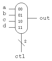 ctl | out Note that "ctl" is a two bit signal, shown by the "2"
----+----
0 0 | a The truth table does not have to expand
0 1 | b a, b, c and d because the mux just passes
1 0 | c the values through to "out" based on the
1 1 | d value of "ctl"
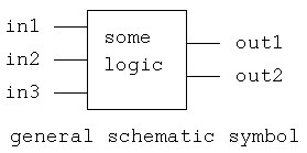
For a general circuit that has some type of description, we use
a rectangle with some notation indicating the function of the
circuit. The inputs and outputs are given signal names.

<- previous index next ->

 A mosfet dynamic ram, one transistor and one capacitor.
The capacitor must be refreshed often. RAS mode:
 Mosfet dynamic ram CAS mode:
 Recent generations of DRAM chips contain an integral refresh counter,
and the memory control circuitry can either use this counter or provide
a row address from an external counter. These chips have three standard
ways to provide refresh, selected by different patterns of signals on the
"column select" (CAS) and "row select" (RAS) lines.
"RAS only refresh" - In this mode the address of the row to refresh
is provided by the address bus lines, so it is used with external
counters in the memory controller.
"CAS before RAS refresh" (CBR) - In this mode the on-chip counter keeps
track of the row to be refreshed and the external circuit merely
initiates the refresh cycles. This mode uses less power because the memory
address bus buffers don't have to be powered up. It is used in most modern
computers.
"Hidden refresh" - This is an alternate version of the CBR refresh cycle
which can be combined with a preceding read or write cycle. The refresh
is done in parallel during the data transfer, saving time.
In the latest (2012) generation of chips the "RAS only" mode has been
eliminated, and the internal counter is used to generate refresh.
The chip has an additional "sleep mode", for use when the computer
is in hibernation, in which an on-chip oscillator generates internal
refresh cycles so that the external clock can be shut down.
some review
"Combinational logic" means gates connected together without feedback.
There is no storage of information. Inputs are applied and outputs
are produced. By convention, we draw combinational logic from
inputs on the left to outputs on the right. For large schematic
diagrams this convention is often violated.
When no constraints are given, any of the gates previously
defined can be connected to design a circuit that performs
the stated function.
Example: Design a circuit that has:
an input for tail lights both on
an input for right turn that lets the signal "osc" control right tail light.
an input for left turn that lets the signal "osc" control left tail light.
("osc" will make the light flash on and off as a turn indicator.)
Constraint: use "and" and "or" gates with inversion bubbles allowed
Solution: There are four inputs "tail" "right" "left" and "osc"
There are two outputs "right_light" and "left_light"
The general strategy in design is to work backward from an output.
Yet, as usual, some work from input toward output is also used.
"right_light" must select between "tail" and "osc". Selection
can typically be implemented by "and" gates feeding an "or" gate
with a control signal into one "and" gate and its complement into
the other "and" gate.
 Analyzing this circuit, if "right" is off, "tail" controls
the "right_light". If "right is on, "osc" controls the "right_light".
A common symbol for this circuit is a multiplexor, mux for short.
The same circuit as above is usually drawn as the schematic diagram:
 Now we can use the first schematic with new labeling for
the "left_light", combining the circuits yields:
 Now a new requirement is added, the flashers must over ride all
other signals and make "osc" drive both right and left tail lights.
A typical design technique is to build on existing designs,
thus note that "flash" only needs to be able to turn on both
the old "right" and old "left". This is two "or" functions
that are easily added to the previous circuit.
 In general a multiplexor can have any number of inputs.
Typically the number of inputs is a power of two and the
control signal, ctl, has the number of bits in the power.
 ctl | out Note that "ctl" is a two bit signal, shown by the "2"
----+----
0 0 | a The truth table does not have to expand
0 1 | b a, b, c and d because the mux just passes
1 0 | c the values through to "out" based on the
1 1 | d value of "ctl"
For a general circuit that has some type of description, we use
a rectangle with some notation indicating the function of the
circuit. The inputs and outputs are given signal names.
