<- previous index next ->
Sequential logic can be represented as three equivalent forms:
State Transition Table, State Transition Diagram and logic circuit.
A State is given a name, we use A, B, C for this discussion, yet
meaningful names are better. A machine or sequential logic circuit
can be in only one state at a time. We are assuming synchronous
logic where all flip flops are clocked by the same clock signal.
The input signal is assumed to be available just before each clock
transition. Optionally, the arrival of an input can also cause the
clock to have one pulse.
Two possible forms of State Transition Table are:
Input state state
| 0 | 1 Input
--+---+--- A 0 B
state A | B | C A 1 C
B | C | B B 0 C
C | C | A B 1 B
C 0 C
C 1 A
The meaning of both tables is:
When in state A with input 0 transition to state B
When in state A with input 1 transition to state C
When in state B with input 0 transition to state C
When in state B with input 1 stay in state B
etc.
The exact same information can be presented as a
State Transition Diagram.
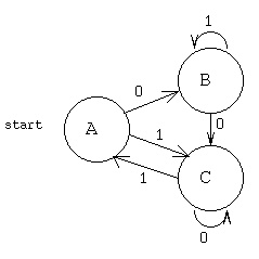 The meaning is the same:
When in state A with input 0 transition to state B
When in state A with input 1 transition to state C
When in state B with input 0 transition to state C
When in state B with input 1 stay in state B
etc.
To convert either a State Transition Table or Diagram to
a circuit, assign a D flip flop to each state. The "q" output
of the flip flop is assigned the signal name of the state.
The "d" input of the flip flop is assigned a signal name
of the state concatenated with "in".
Write the combinational logic equations for each state
input from observing the "to" state in the transition table
or diagram.
For this sequential machine, using I as the input
Ain <= (C and I); -- C transitions to A when I='1'
Bin <= (A and not I) or -- A transitions to B when I='0'
(B and I); -- B transitions to B when I='1'
Cin <= (A and I) or -- A transitions to C when I='1'
(B and not I) or -- B transitions to C when I='0'
(C and not I); -- C transitions to C when I='0'
The partial circuit is shown below.
Implied is a set signal to A and reset signals to
B and C for the initial or start condition.
Implied is a common clock signal to all flip flops.
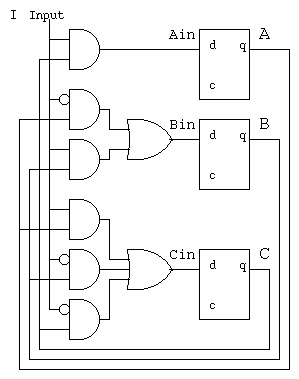 Not shown is the output(s) that may be any combinational
circuit, function, of the input and states.
e.g. out <= (A and I) or (B and not I);
There is an algorithm and corresponding computer program for
minimizing the State Transition Table,
see Myhill Nerode minimization.
There is an algorithm and corresponding computer program for
minimizing the combinational logic
are Quine McClusky minimization.
One application of sequential logic is for garage door openers
or car door locks. The basic sequential logic is a spin lock.
This circuit has the property of eventually detecting the
specific sequence it is designed to accept. The transmitter may
start anywhere in the sequence and continue to repeat the sequence
until the receiver detects the specific sequence.
 state | input from rcvr
| 0 | 1 |
------+---+---+
A | A | B |
B | C | A |
C | A | D |
D | A | E |
E | F | A |
F | A | A activate signal
This "spin lock" is designed to accept the sequence 101101.
A logic circuit, by inspection of the state transition table
using I for input from rcvr, DFF outputs are DFF name,
DFF D input is DFF name with "in".
Ain = (~I&A)|(I&B)|(~I&C)|(~I&D)|(I&E)|F
Bin = ( I&A)
Cin = (~I&B)
Din = (I&C)
Ein = (I&D)
Fin = (~I&E)
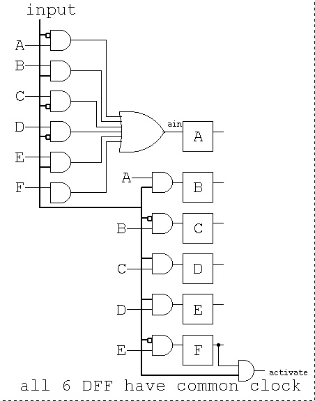 A transmitter could be designed to send the specific sequence
followed by an equal number of zero bits then repeat the
specific sequence. (Assuming the first bit of the sequence is a '1')
An all zero code is not useful.
More sophisticated spin locks will change the sequence that is
detected each time a sequence is accepted. The transmitter must then
send a family of sequences because, in general, the transmitter
will not know what the receivers sequence setting is. A method
of handling this unknown is to have the receiver change to a
pseudo random setting of some of the bit positions. The
transmitter then generates and transmits all of the pseudo random
patterns in the correct bit positions. Sample pseudo random
sequence generators are shown below.
A maximal length pseudo random sequence generator can generate
2^n -1 unique patterns with an n-bit shift register. For each
number of shift register stages there are one or more feedback
circuits using just exclusive-or to compute the next input bit.
The output may be n-bit patterns, a2, a1. a0 in the circuit below.
The output may also be a bit stream taken from just a0 or a2.
The basic shift register is clocked at some frequency. Bits shift
left to right one position per clock. The top bit is inserted
based on the feedback into the exclusive-or gate(s).
A sequence, starting with the "seed" 0 0 1 is shown below:
 0 0 1
1 0 0
0 1 0
1 0 1
1 1 0
1 1 1
0 1 1
0 0 1
Notice the 2^3 -1 = 7 unique patterns and then the repeat.
A maximal length pseudo random shift register for 5-bit patterns is
shown in typical abbreviated schematic form.
0 0 1
1 0 0
0 1 0
1 0 1
1 1 0
1 1 1
0 1 1
0 0 1
Notice the 2^3 -1 = 7 unique patterns and then the repeat.
A maximal length pseudo random shift register for 5-bit patterns is
shown in typical abbreviated schematic form.
 With a seed of 0 0 0 0 1 the next few values are
1 0 0 0 0
1 1 0 0 0
1 1 1 0 0
0 1 1 1 0
The full output sequence with bits reversed
Maximal length pseudo random sequences may be generated for
any length. Below in short hand notation is the feedback paths
for many lengths up to 32.
/* length bits(high order first) of h[], right is h[0]
* 2 1 1 1 top bit always one, the input to msb stage
* 3 1 0 1 1 bottom bit always one, output of lsb stage
* 4 1 0 0 1 1 x(4)= x^1+x^0 x^0=1 initially
* 5 1 1 0 1 1 1 x(5)=x^4+x^2+x^1+x^0 x^0=1 initially
* 6 1 0 0 0 0 1 1 + is exclusive or
* 7 1 1 1 1 0 1 1 1 x^0 is rightmost bit
* 8 1 1 1 1 0 0 1 1 1 x^1 is next bit, etc.
* 9 1 1 1 0 0 0 1 1 1 1
* 10 1 1 0 0 1 1 1 1 1 1 1
* 11 1 1 0 1 1 0 0 1 1 1 1 1
* 12 1 1 0 0 0 1 0 0 1 0 1 1 1
* 13 1 1 0 0 0 1 1 1 1 1 1 1 1 1
* 14 1 1 0 1 0 0 0 1 1 1 1 1 1 1 1
* 15 1 1 0 1 0 0 0 1 1 0 1 1 1 1 1 1
* 16 1 1 0 1 1 0 0 0 0 0 1 1 1 1 1 1 1
* 18 1 1 1 1 0 0 0 0 1 1 0 0 0 1 1 0 0 0 1
* 20 1 1 0 0 0 0 0 0 0 0 0 0 0 0 0 0 1 1 0 0 1
* 24 1 0 0 0 0 0 0 0 0 0 0 0 0 0 0 0 0 1 0 0 0 0 1 1 1
* 30 1 0 0 0 0 0 0 1 0 0 0 0 0 0 0 0 0 0 0 0 0 0 0 0 0 0 0 0 1 1 1
* 31 1 0 0 0 1 0 0 0 1 0 0 0 1 0 0 0 1 0 0 0 1 1 1 0 1 1 1 0 1 1 1 1
* 32 1 0 0 0 0 0 1 0 0 1 1 0 0 0 0 0 1 0 0 0 1 1 1 0 1 1 0 1 1 0 1 1 1
*/
project 5 you will finish a spin lock:
see project 5 spin lock.
<- previous index next ->
 The meaning is the same:
When in state A with input 0 transition to state B
When in state A with input 1 transition to state C
When in state B with input 0 transition to state C
When in state B with input 1 stay in state B
etc.
To convert either a State Transition Table or Diagram to
a circuit, assign a D flip flop to each state. The "q" output
of the flip flop is assigned the signal name of the state.
The "d" input of the flip flop is assigned a signal name
of the state concatenated with "in".
Write the combinational logic equations for each state
input from observing the "to" state in the transition table
or diagram.
For this sequential machine, using I as the input
Ain <= (C and I); -- C transitions to A when I='1'
Bin <= (A and not I) or -- A transitions to B when I='0'
(B and I); -- B transitions to B when I='1'
Cin <= (A and I) or -- A transitions to C when I='1'
(B and not I) or -- B transitions to C when I='0'
(C and not I); -- C transitions to C when I='0'
The partial circuit is shown below.
Implied is a set signal to A and reset signals to
B and C for the initial or start condition.
Implied is a common clock signal to all flip flops.
 Not shown is the output(s) that may be any combinational
circuit, function, of the input and states.
e.g. out <= (A and I) or (B and not I);
There is an algorithm and corresponding computer program for
minimizing the State Transition Table,
see Myhill Nerode minimization.
There is an algorithm and corresponding computer program for
minimizing the combinational logic
are Quine McClusky minimization.
One application of sequential logic is for garage door openers
or car door locks. The basic sequential logic is a spin lock.
This circuit has the property of eventually detecting the
specific sequence it is designed to accept. The transmitter may
start anywhere in the sequence and continue to repeat the sequence
until the receiver detects the specific sequence.
 state | input from rcvr
| 0 | 1 |
------+---+---+
A | A | B |
B | C | A |
C | A | D |
D | A | E |
E | F | A |
F | A | A activate signal
This "spin lock" is designed to accept the sequence 101101.
A logic circuit, by inspection of the state transition table
using I for input from rcvr, DFF outputs are DFF name,
DFF D input is DFF name with "in".
Ain = (~I&A)|(I&B)|(~I&C)|(~I&D)|(I&E)|F
Bin = ( I&A)
Cin = (~I&B)
Din = (I&C)
Ein = (I&D)
Fin = (~I&E)
 A transmitter could be designed to send the specific sequence
followed by an equal number of zero bits then repeat the
specific sequence. (Assuming the first bit of the sequence is a '1')
An all zero code is not useful.
More sophisticated spin locks will change the sequence that is
detected each time a sequence is accepted. The transmitter must then
send a family of sequences because, in general, the transmitter
will not know what the receivers sequence setting is. A method
of handling this unknown is to have the receiver change to a
pseudo random setting of some of the bit positions. The
transmitter then generates and transmits all of the pseudo random
patterns in the correct bit positions. Sample pseudo random
sequence generators are shown below.
A maximal length pseudo random sequence generator can generate
2^n -1 unique patterns with an n-bit shift register. For each
number of shift register stages there are one or more feedback
circuits using just exclusive-or to compute the next input bit.
The output may be n-bit patterns, a2, a1. a0 in the circuit below.
The output may also be a bit stream taken from just a0 or a2.
The basic shift register is clocked at some frequency. Bits shift
left to right one position per clock. The top bit is inserted
based on the feedback into the exclusive-or gate(s).
A sequence, starting with the "seed" 0 0 1 is shown below:
 0 0 1
1 0 0
0 1 0
1 0 1
1 1 0
1 1 1
0 1 1
0 0 1
Notice the 2^3 -1 = 7 unique patterns and then the repeat.
A maximal length pseudo random shift register for 5-bit patterns is
shown in typical abbreviated schematic form.
0 0 1
1 0 0
0 1 0
1 0 1
1 1 0
1 1 1
0 1 1
0 0 1
Notice the 2^3 -1 = 7 unique patterns and then the repeat.
A maximal length pseudo random shift register for 5-bit patterns is
shown in typical abbreviated schematic form.
 With a seed of 0 0 0 0 1 the next few values are
1 0 0 0 0
1 1 0 0 0
1 1 1 0 0
0 1 1 1 0
The full output sequence with bits reversed
Maximal length pseudo random sequences may be generated for
any length. Below in short hand notation is the feedback paths
for many lengths up to 32.
/* length bits(high order first) of h[], right is h[0]
* 2 1 1 1 top bit always one, the input to msb stage
* 3 1 0 1 1 bottom bit always one, output of lsb stage
* 4 1 0 0 1 1 x(4)= x^1+x^0 x^0=1 initially
* 5 1 1 0 1 1 1 x(5)=x^4+x^2+x^1+x^0 x^0=1 initially
* 6 1 0 0 0 0 1 1 + is exclusive or
* 7 1 1 1 1 0 1 1 1 x^0 is rightmost bit
* 8 1 1 1 1 0 0 1 1 1 x^1 is next bit, etc.
* 9 1 1 1 0 0 0 1 1 1 1
* 10 1 1 0 0 1 1 1 1 1 1 1
* 11 1 1 0 1 1 0 0 1 1 1 1 1
* 12 1 1 0 0 0 1 0 0 1 0 1 1 1
* 13 1 1 0 0 0 1 1 1 1 1 1 1 1 1
* 14 1 1 0 1 0 0 0 1 1 1 1 1 1 1 1
* 15 1 1 0 1 0 0 0 1 1 0 1 1 1 1 1 1
* 16 1 1 0 1 1 0 0 0 0 0 1 1 1 1 1 1 1
* 18 1 1 1 1 0 0 0 0 1 1 0 0 0 1 1 0 0 0 1
* 20 1 1 0 0 0 0 0 0 0 0 0 0 0 0 0 0 1 1 0 0 1
* 24 1 0 0 0 0 0 0 0 0 0 0 0 0 0 0 0 0 1 0 0 0 0 1 1 1
* 30 1 0 0 0 0 0 0 1 0 0 0 0 0 0 0 0 0 0 0 0 0 0 0 0 0 0 0 0 1 1 1
* 31 1 0 0 0 1 0 0 0 1 0 0 0 1 0 0 0 1 0 0 0 1 1 1 0 1 1 1 0 1 1 1 1
* 32 1 0 0 0 0 0 1 0 0 1 1 0 0 0 0 0 1 0 0 0 1 1 1 0 1 1 0 1 1 0 1 1 1
*/
project 5 you will finish a spin lock:
see project 5 spin lock.