 These are not intended to be complete lecture notes.
 Complicated figures or tables or formulas are included here
 in case they were not clear or not copied correctly in class.
 Computer commands, directory names and file names are included.
 Specific help may be included here yet not presented in class.
 Source code may be included in line or by a link.

 Lecture numbers correspond to the syllabus numbering.
Introduction:
  Hello, my name is Jon Squire and I have been programming
  computers since 1959. I have served my time in corporate
  management for 25 years. This course covers a little history
  of computer architecture through some of the latest advances
  and practical information you may use in buying, upgrading or
  building your own computer.

  After this course, you can say that you have performed
  "modeling and simulation" possibly a valuable asset in finding
  a job. You will be skilled in converting graphical and schematic
  information to textual information and the reverse.

Some Brief History:
  The ISA card slots were replaced by PCI card slots that
  are replaced by external USB devices. The
  serial port for RS232 devices is replaced by the USB port.
  Floppy disk are disappearing along with that connector on
  the motherboard. RAM still uses DIMM's and the slots have
  grown to handle 4, 8 and 16 gigabytes of memory. ATA hard
  drives are replaced by SATA hard drives, 5TB and more available.
  Some rotating hard drives are being replaced by SSD, solid
  state drives. The printer port will be going as will the
  AGP graphics connector. HDMI and now DP. That expensive graphics
  card you bought will probably not work in your new computer.

  I have been saving architecture news.

Overview:
  This course will present detailed information on the internal
  working of the CPU, cache, memory, busses and peripheral devices
  such as disk drives and DVD's. The course five part project will
  have each student simulate a small computer using the VHDL
  digital simulation language. Either Cadence VHDL or free GHDL.

  Read the syllabus.

All of the lectures are covered in these WEB pages.
Lecture notes are often updated. (You may ask questions.)
And, sometimes corrected after questions.
Some information is still presented on the blackboard/whiteboard.

Check UMBC "Blackboard" for announcements and grades.

The Top 500 Multiprocessor systems are evaluated about every six
months. These are not your typical home computers.

  The Top 10 are shown www.top500.org/lists/2020/06
  As many as 10  million cores! (How many in your computer?)


More Lecture 1, pdf format

The free market system and resulting competition, provide better and
more economical products to consumers. Expect flip-flop between
vendors for best or most economical products.


A standard engineering statement is:
Fast, Cheap, Reliable - pick any two.

Monopolies: Ford Motor Company, Standard Oil of New Jersey, IBM, AT&T, ...
Microsoft.

Computer Architecture Development:
System Architecture


Logic Design


Circuit Design


Device Physics
For the inverter above, a chip cross section is:


N type and P type impurities are diffused into the silicon substrate
through a mask, typically in a high temperature vacuum process.

Oh! Oh! It is now predicted that Moore's Law:
The gate width of transistors will halve every 18 months,
will end in 2021. Prior estimates ended in 2028.
Never fear, monolithic 3D is here.

Mask Making and Processing


The black would be a metalization mask, here showing the
transistor input connection. Other masks are for P+, N+,
N well and via (the etch through the SiO2 to allow electrical
connection to metal.)


The large round wafer, after processing with all the masks,
is broke up into many rectangular dies. Each die is placed
in a package and the input and output pads on the die are
connected to the pins on the package. The die in the package
is called a chip or IC chip or Integrated Circuit Chip.


"Feature size" is the smallest dimension of metal width, gate width,
metal spacing, etc. coming 12 nanometers is 0.000 000 012 meter or
less than 1 millionth of an inch.


This gets smaller every year or so.

BYOC
Build your own computer


I have built several computers buying a case,
motherboard, cpu, ram, drives, video, audio.

My older desktop, AMD FX 8-core is Cybertron G1244A
16 GB ram, 1/2 TB SDD.
(Replacing my old 12 core AMD that is acting up.)
Now new Dell Precision 7920 Tower with 16 cores.

You want DDR3, SATA3, SSD  we will cover these in future lectures.


Look at Homework 1, it is assigned today.
The best method of measuring a computers performance
is to use benchmarks. Some suggestions from my
personal experience preparing a benchmark suite
and several updates and personal benchmark
experience are presented in pdf format.


Lecture 2

Smaller time is better, higher clock frequency is better.
time = 1 / frequency   T = 1/F   and  F = 1/T
1 picosecond =  1 / 1 THz
1 nanosecond =  1 / 1 GHz
1 microsecond = 1 / 1 MHz
1 millisecond = 1 / 1 Khz

kilohertz KHz = 10^3  cycles per second clock
megahertz MHz = 10^6  cycles per second clock
gigahertz GHz = 10^9  cycles per second clock
terahertz THz = 10^12 cycles per second clock

Definitions:
CPI    Clocks Per Instruction
MHz    Megahertz, millions of cycles per second
MIPS   Millions of Instructions Per Second = MHz / CPI
MOPS   Millions of Operations Per Second
MFLOPS Millions of Floating point Operations Per Second
MIOPS  Millions of Integer Operations Per Second


Do not trust your computers clock or the software
that reads and processes the time.

First: Test the wall clock time against your watch.

time_test.c
time_test.java
time_test.py
time_test.f90

The program displays 0, 5, 10, 15 ... at 0 seconds,
5 seconds, 10 seconds etc.

demonstrate time_test if possible


Note the use of <time.h> and 'time()'

Beware, midnight is zero seconds.
Then 60 sec/min * 60 min/hr * 24 hr/day = 86,400 sec/day
Just before midnight is 86,399 seconds.
Running a benchmark across midnight may give a negative time.


Then: Test CPU time, this should be just the time
used by the program that is running. With only
this program running, checking against your watch
should work.

time_cpu.c
time_cpu.java
time_cpu.py

The program displays 0, 5, 10, 15 ... at 0 seconds,
5 seconds, 10 seconds etc.

Note the use of <time.h> and
  '(double)clock()/(double)CLOCKS_PER_SEC'

I have found one machine with the constant
CLOCKS_PER_SECOND completely wrong and
another machine with a value 64 that should
have been 100. A computer used for real time
applications could have a value of 1,000,000
or more.

More graphs of FFT benchmarks


The source code, C language, for the FFT benchmarks:

Note the check run to be sure the code works.

Note the non uniform data to avoid special cases.

fft_time.c main program
fftc.h header file

FFT and inverse FFT for various numbers of complex data points
The same source code was used for all benchmark measurements.
These were optimized for embedded computer use where all
constants were burned into rom.

fft16.c   ifft16.c
fft32.c   ifft32.c
fft64.c   ifft64.c
fft128.c  ifft128.c
fft256.c   ifft256.c
fft512.c   ifft512.c
fft1024.c ifft1024.c
fft2048.c ifft2048.c
fft4096.c ifft4096.c

Some of the result files:
P1-166MHz
P1-166MHz -O2
P2-266MHz
P2-266MHz -O2
Celeron-500MHz
P3-450MHz MS
P3-450MHz Linux
PPC-2.2GHz
PPC-2.5GHz
P4-2.53GHz XP
Alpha-533MHz XP
Xeon-2.8GHz
Athlon-1.4GHz MS
Athlon-1.4GHz XP
Athlon-1.4GHz SuSe
Laptop Win7
Laptop Ubuntu


What if you are benchmarking a multiprocessor?
For example, a two core or quad core, then use both CPU time
and wall time to get average processor loading:

time_mp2.c for two cores
time_mp4.c for quad cores
time_mp8.c for two quad cores
time_mp12.c for two six cores
The output from a two cores is:
time_mp2_c.out for two core Xeon
The output from four cores is:
time_mp4_c.out for Mac quad G5
The output from eight cores is:
time_mp8_c.out for AMD 12-core
The output from twelve cores is:
time_mp12_c.out for AMD 12-core

end of time_mp12_c.out file:
  total CPU time is 342.970000 seconds
  wall time is 29.000000 seconds
  average number of processors used = 11.826552
  time_mp12.c exiting

Similar tests in Java
time_test.java
time_cpu.java
time_mp4.java for quad cores
time_mp8.java for eight cores
time_mp8.java for eight and twelve cores
time_mp4_java.out for quad Xeon G5
time_mp8_java.out for 8 thread Xeon G5
time_mp8_java_fx.out for 8 core AMD FX
time_mp12_java.out for 8 thread Xeon G5
time_mp12_12_java.out for 12 core AMD
matmul_thread4.java
matmul_thread4_java.out

Time_test and threads in Python
time_test.py
time_cpu.py
parallel_matmul.py
parallel_matmul_py.out


OK, since these were old and I did not want to change them,
they give some indications of performance on various machines
with various operating systems and compiler options.

To measure very short times, a higher quality, double-difference
method is needed. The following program measures the time
to do a double precision floating point add. This may be
a time smaller than 1ns, 10^-9 seconds.

A test harness is needed to calibrate the loops and make sure
dead code elimination can not be used by the compiler.

The the item to be tested is placed in a copy of the test harness
to make the measurement.

The time of the test harness is the stop minus start time in seconds.

The time for the measurement is the stop minus start time in seconds.

The difference, thus double difference, between the harness and
measurement is the time for the item being measured.
Here A = A + B with B not known to be a constant by the compiler,
is reasonably expected to be a single instruction to add B to
a register. If not, we have timed the full statement.

The double difference time must be divided by the total
number of iterations from the nested loops to get the
time for the computer to execute the item once.

An attempt is made to get a very stable time measurement.
Doubling the number of iterations should double the time.

Summary of double difference
  t1 saved
  run test harness
  t2 saved

  t3 saved
  run measurement, test harness with item to be timed
  t4 saved
  tdiff = (t4-t3) - (t2-t1)
  t_item = tdiff / number of iterations

  check against previous time, if not close, double iterations

The source code is:

time_fadd.c
fadd on P4 2.53GHz
fadd on Xeon 2.66GHz
fadd on Mac 2.5GHz

end of Mac output:
  time_fadd.c
  ...
  rep=16384, t measured=0.814363
  rep=32768, t measured=1.62344
  rep=65536, t measured=3.28666
  tmeas=3.28666, t_prev=0, rep=65536
  rep=65536, t measured=3.28829
  tmeas=3.28829, t_prev=3.28666, rep=65536
  time measured=3.28829, under minimum
  raw time=3.28829, fadd time=5.01629e-10, rep=65536, stable=0.000497342


Some extra information for students wanting to explore their computer:

Windows OS                               Linux OS

What is in my computer?
  start                                  cd /proc
    control panel                        cat cpuinfo
      system
        device manager
          processor
          etc.

What processes are running in my computer?
  ctrl-alt-del                           ps -el
    process                              top

How do I easily time a program?
  command prompt                         time prog < input > output
    time

    prog < input > output
    time


The time available through normal software calls may be
updated less than 30 times per second to more than a
million times per second. A general rule of thumb is to
have the time being measured be 10 seconds or more. This
will give a reasonable accurate time measurement on all
computers. Just repeat what is being measured if it does
not run 10 seconds.

Some history about computer time reporting.
There were time sharing system where you bought time on
the computer by the cpu second. There is the cpu time
your program requires that is usually called your process
time. There is also operating system cpu time. When there
are multiple processes running, the operating system
time slices, running each job for a short time, called
a quanta. The operating system must manage memory, devices,
scheduling and related tasks. In the past we had to keep
a very close eye on how cpu time was charged to the users
process verses the systems processes and was "dead time"
the idle process, charged to either. From a users point
of view, the user did not request to be swapped out, thus
the user does not want any of the operating system time
for stopping and restarting the users process to be
charged to the user.

Another historic tidbit, some Unix systems would add
one microsecond to the time reported on each system
request for the time. Never allowing the same time
to be reported twice even if the clock had not
updated. This was to ensure that all disk file times
were unique and thus programs such as 'make' would
be reliable.

For more recent SPEC benchmarks,  2006 is suit date, run 2015,2016,2017,2018,2019,2020

see CPU integer benchmarks,SPECint,  floating point benchmarks,SPECfp
www.spec.org/cpu2006/Docs/


Some times you just have to buy the top of the line and forget benchmarks.


Now find a display with 2,560 by 2,048 resolution!
(other than the NASA display)


Newegg has an Acer 22 inch HDMI 1920 by 1080 for under $100 in 2013
HDMI replaces VGA connection from computer to display.
  Repeating some definitions:
  CPI    Clocks Per Instruction
  MHz    megahertz, millions of cycles per second
  MIPS   Millions of Instructions Per Second = MHz / CPI
  MOPS   Millions of Operations Per Second
  MFLOPS Millions of Floating point Operations Per Second
  MIOPS  Millions of Integer Operations Per Second
  (Classical, old, terms. Today would be billions.)

  Amdahl's Law (many forms, understand the concept)

             the part of time improved
  new time = -------------------------  +  the part of time not improved
             factor improved by

  old time = the part of time improved + the part of time not improved

            old time
  speedup = --------     (always bigger over smaller when faster)
            new time

  Given: on some program, the CPU takes 9 sec and the disk I/O takes 1 sec
         What is the speedup using a CPU 9 times faster?
                     9 sec
  Answer: new time = ----- + 1 sec = 2 sec
                       9

          old time = 9 + 1 = 10 sec

          speedup = 10 / 2 = 5   a pure number

------------------------------------------------------------------------------

  Amdahl's Law (many forms, understand the concept)

             new performance
   speedup = ---------------
             old performance

   Given: Performance of M1 is 100 MFLOPS and 200 MIOPS
          Performance of M2 is  50 MFLOPS and 250 MIOPS
          On a program using 10% floating point and 90% integer
          Which is faster?  What is the speedup?

   Answer; .1 * 100 + .9 * 200 = 190 MIPS
           .1 *  50 + .9 * 250 = 230 MIPS   (M2 is faster)

           speedup = 230/190 = 1.21
------------------------------------------------------------------------------

                                     old performance
   new performance = -----------------------------------------------------
                     fraction of old improved
                     ------------------------ + fraction of old unimproved
                      improvement factor

   Given: half of a 100 MIPS machine is speeded up by a factor of 3
          what is the speedup relative to the original machine?
                                 1                    1
   Answer: new performance = --------- * 100 MIPS = ---- * 100 MIPS = 150 MIPS
                             0.5                    .666
                             --- + 0.5
                              3
                                                         1
           speedup = 150 / 100 = 1.5 (same as -------------------------------)
                                              fraction improved
                                              ------------------ + fraction
                                              improvement factor    unimproved

speedup is a pure number, no units. The units must cancel.

------------------------------------------------------------------------------

SPEC Benchmarks

The benchmarks change infrequently, for example  2006 - 2016 same
The speed seems to increase every year.

SPEC Int2006, 9 in C, 3 in C++

SPEC Flt2006, 17 in assorted Fortran, C, C++

SPEC many rules to follow

recent int results
recent flt results
Note number of core available, results seem to be using just one core.

------------------------------------------------------------------------------

CPI is average Clocks Per Instruction. units: clock/inst
MHz is frequency, we use millions of clocks per second. units: clock/sec
MIPS is millions of instruction per second. units: inst/sec
Note: MIPS=MHz/CPI  because  (clock/sec) / (clock/inst) = 10^6 inst/sec
( 5/4 of people do not understand fractions. )


                  Computing average CPI, Clocks Per Instruction

     -------given---------------    ----------compute------------

     type  clocks  %use             product

     RR      3      25%             3 * 25 =  75
     RM      4      50%             4 * 50 = 200
     MM      5      25%             5 * 25 = 125
                 ______                     ____
                   100%                      400    sum

                                    400/100 = 4 average CPI


     -------given---------------    ----------compute------------

     type  clocks  instructions     product
     RR      3       25,000         3 * 25,000 =  75,000
     RM      4       50,000         4 * 50,000 = 200,000
     MM      5       25,000         5 * 25,000 = 125,000
                    _______                      _______
                    100,000                      400,000     sum

                                    400,000/100,000 = 4 average CPI

     Find the faster sequence of instructions  Prog1 vs Prog2

     -------given---------------------

     type    clocks
      A        1
      B        2
      C        3

     instruction counts for  A   B   C
     Prog1                   2   1   2
     Prog2                   4   1   1

     ----------compute------------------------------
     Prog1
     A    1   2     1 * 2 = 2
     B    2   1     2 * 1 = 2
     C    3   2     3 * 2 = 6
                           __ sum
                           10 clocks

     Prog2
     A    1   4     1 * 4 = 4
     B    2   1     2 * 1 = 2
     C    3   1     3 * 1 = 3
                           __ sum
                            9 clocks   more instructions yet faster

     speedup = 10 clocks / 9 clocks = 1.111   a number (no units)


cs411_opcodes.txt different from Computer Organization and Design  1/8/2020

rd is register destination, the result, general register 1 through 31
rs is the first register,  A, source, general register 0 through 31
rt is the second register, B, source, general register 0 through 31

--val---- generally a 16 bit number that gets sign extended
--adr---- a 16 bit address, gets sign extended and added to (rx)
"i" is generally immediate, operand value is in the instruction

Opcode Operands    Machine code format
                       6   5   5   5   5   6  number of bits in field

nop                RR  00  0   0   0   0   00
add    rd,rs,rt    RR  00  rs  rt  rd  0   32
sub    rd,rs,rt    RR  00  rs  rt  rd  0   34
mul    rd,rs,rt    RR  00  rs  rt  rd  0   27
div    rd,rs,rt    RR  00  rs  rt  rd  0   24
and    rd,rs,rt    RR  00  rs  rt  rd  0   13
or     rd,rs,rt    RR  00  rs  rt  rd  0   15
srl    rd,rt,shf   RR  00  0   rt  rd  shf 03
sll    rd,rt,shf   RR  00  0   rt  rd  shf 02
cmpl   rd,rt       RR  00  0   rt  rd  0   11
j      jadr        J   02  ------jadr--------
lwim   rd,rs,val   M   15  rs  rd  ---val----
addi   rd,rs,val   M   12  rs  rd  ---val----
beq    rs,rt,adr   M   29  rs  rt  ---adr----
lw     rd,adr(rx)  M   35  rx  rd  ---adr----
sw     rt,adr(rx)  M   43  rx  rt  ---adr----


        instruction bits (binary of 6 5 5 5 5 6 format above)
 3 3 2 2 2 2 2 2 2 2 2 2 1 1 1 1 1 1 1 1 1 1
 1 0 9 8 7 6 5 4 3 2 1 0 9 8 7 6 5 4 3 2 1 0 9 8 7 6 5 4 3 2 1 0
            |         |         |         |         |
 0 0 0 0 0 0 0 0 0 0 0 0 0 0 0 0 0 0 0 0 0 0 0 0 0 0 0 0 0 0 0 0 nop

 0 0 0 0 0 0 a a a a a b b b b b r r r r r -ignored- 1 0 0 0 0 0 add r,a,b

 0 0 0 0 0 0 a a a a a b b b b b r r r r r -ignored- 1 0 0 0 1 0 sub r,a,b

 0 0 0 0 0 0 a a a a a b b b b b r r r r r -ignored- 0 1 1 0 1 1 mul r,a,b

 0 0 0 0 0 0 a a a a a b b b b b r r r r r -ignored- 0 1 1 0 0 0 div r,a,b

 0 0 0 0 0 0 a a a a a b b b b b r r r r r -ignored- 0 0 1 1 0 1 and r,a,b

 0 0 0 0 0 0 a a a a a b b b b b r r r r r -ignored- 0 0 1 1 1 1 or  r,a,b

 0 0 0 0 0 0 0 0 0 0 0 b b b b b r r r r r s s s s s 0 0 0 0 1 1 srl r,b,s

 0 0 0 0 0 0 0 0 0 0 0 b b b b b r r r r r s s s s s 0 0 0 0 1 0 sll r,b,s

 0 0 0 0 0 0 0 0 0 0 0 b b b b b r r r r r -ignored- 0 0 1 0 1 1 cmpl r,b

 0 0 0 0 1 0 -----address to bits (27:2) of PC------------------ j adr

 0 0 1 1 1 1 x x x x x r r r r r ---2's complement value-------- lwim r,val(x)

 0 0 1 1 0 0 x x x x x r r r r r ---2's complement value-------- addi r,val(x)

 0 1 1 1 0 1 a a a a a b b b b b ---2's complement address------ beq a,b,adr

 1 0 0 0 1 1 x x x x x r r r r r ---2's complement address------ lw r,adr(x)

 1 0 1 0 1 1 x x x x x b b b b b ---2's complement address------ sw b,adr(x)


 Definitions:
 nop          no operation, no programmer visible registers or memory
              are changed, except PC gets PC+4

 j adr        bits 0 through 25 of the instruction are inserted into PC(27:2)
              probably should zero bits PC(1:0) but should be zero already

 lw r,adr(x)  load word into register r from memory location (register x plus
              sign extended adr field)

 sw b,adr(x)  store word from register b into memory location (register x plus
              sign extended adr field)

 beq a,b,adr  branch on equal, if the contents of register a are equal
              to the contents of register b, add the, shifted by two,
              sign extended adr to the PC (The PC will have 4 added by then)

 lwim r,val(x) load immediate, the contents of register x is added to the
              sign extended value and the result put into register r

 addi r,val(x) add immediate, the contents of register x is added to the
              sign extended value and the result added to register r

 add r,a,b    add register a to register b and put result into register r

 sub r,a,b    subtract register b from register a and put result into register r

 mul r,a,b    multiply register a by register b and put result into register r

 div r,a,b    divide register a by register b and put result into register r

 and r,a,b    and register a to register b and put result into register r

 or  r,a,b    or register a to register b and put result into register r

 srl r,b,s    shift the contents of register b by s places right and put
              result in register r

 sll r,b,s    shift the contents of register b by s places left and put
              result in register r

 cmpl r,b     one's complement of register b goes into register r

 Also: no instructions are to have side effects or additional "features"


General register list (applies to MIPS ISA and project)
                      (note: project op codes may differ from MIPS/SGI)

Register          notes
 0   $0           zero value, not writable
 1   $1
 2   $2   $v0     return values (convention, not constrained by hardware)
 3   $3   $v1
 4   $4   $a0     arguments (convention, not constrained by hardware)
 5   $5   $a1
 6   $6   $a2
 7   $7   $a3
 8   $8   $t0     temporaries(not saved by software convention over calls)
 9   $9   $t1
10   $10  $t2
11   $11  $t3
12   $12  $t4
13   $13  $t5
14   $14  $t6
15   $15  $t7
16   $16  $s0     saved by software convention over calls
17   $17  $s1
18   $18  $s2
19   $19  $s3
20   $20  $s4
21   $21  $s5
22   $22  $s6
23   $23  $s7
24   $24  $t8     more temporaries
25   $25  $t9
26   $26
27   $27
28   $28  $gp     global pointer ( more designations by software convention)
29   $29  $sp     stack pointer
30   $30  $fp     frame pointer
31   $31  $ra     return address

Remember: From a hardware view registers 1 through 31 are general purpose
and identical. The above table is just software conventions.
Register zero is always zero!

Basic digital logic

IA-64 Itanium


We will cover multicore and parallel processors later.
Amdahls law applies to them also.


HW2 assignment
We now look at instructions in memory, how they got there and
how they execute:
1. Start by using an editor to enter compiler language statements.
The editor writes your source code to a disk file.
2. A compiler reads the source code disk file and produces
assembly language instructions for a specific ISA that
will perform your compiler language statements. The assembly
language is written to a disk file.
3. An assembler reads the assembly language disk file and produces
a relocatable binary version of your program and writes it to
a disk file. This may be a main program or just a function or
subroutine. Typical file name extension is .o or .obj
4. A linkage editor or binder or loader combines the relocatable
binary files into an executable file. Addresses are relocated
and typically all instructions are put sequentially in a code
segment, all constant data in another segment, variables and
arrays in another segment and possibly making other segments.
The addresses in all executable files for a specific computer
start at the same address. These are virtual addresses and the
operating system will place the segments into RAM at other
real memory addresses. Windows file extension .exe
5. A program is executed by having the operating system load the
executable file into RAM and set the program counter to the
address of the first instruction that is to be executed in
the program. All programs might have the same starting address,
yet the operating system has set up the TLB to translate the
virtual instruction and data addresses to physical memory addresses.
The physical addresses are not available to the program or to a
debugger. This is part of the security an operating system
provides to prevent one persons program from affecting another
persons program.
A simple example:
Compiler input int a, b=4, c=7;
a = b + c;
Assembly language fragment (not unique)
lw $2,12($fp) b at 12 offset from frame pointer
lw $3,16($fp) c at 16 offset from frame pointer
add $2,$2,$3 R format instruction
sw $2,8($fp) a at 8 offset from frame pointer
Memory addresses in bytes, integer typically 4 bytes, 32 bits.
Loaded in machine
virtual address content 32-bits 8-hexadecimal digits
00000000 8FC2000C lw $2,12($fp)
00000004 8FC30010 lw $3,16($fp)
00000008 00000000 nop inserted for pipeline
0000000C 00431020 add $2,$2,$3
00000010 AFC20008 sw $2,8,($fp)
$fp has 10000000 (data frame)
10000000 00000000
10000004 00000001
10000008 00000000? a after execution
1000000C 00000004 b
10000010 00000007 c
Instruction field format for add $2,$2,$3
0000 0000 0100 0011 0001 0000 0010 0000 binary for 00431020 hex
vvvv vvss ssst tttt dddd dhhh hhvv vvvv 6,5,5,5,5,6 bit fields
0 | 2 | 3 | 2 | 0 | 32 decimal values of fields
Instruction field format for lw $2,12($fp) $fp is register 30
1000 1111 1100 0010 0000 0000 0000 1100 binary for 8FC2000C hex
vvvv vvxx xxxd dddd aaaa aaaa aaaa aaaa 6,5,5,16 bit fields
35 | 30 | 2 | 12 decimal values of fields
The person writing the assembler chose the format of an assembly
language line. The person designing the ISA chose the format of
the instruction. Why would you expect them to be in the same order?
 A very simplified data flow of the add instruction. From the
registers to the ALU and back to the registers.
A very simplified data flow of the add instruction. From the
registers to the ALU and back to the registers.
 The VHDL to use the ALU will be given to you as:
ALU: entity WORK.alu_32 port map(inA => EX_A,
inB => EX_aluB,
inst => EX_IR,
result => EX_result);
We will call the upper input "A" and the lower input "B"
and the output "result".
The extra input, EX_IR, not shown on the diagram above
is the instruction the ALU is to perform, add, sub, etc.
The instructions we will use in this course are specifically:
cs411_opcodes.txt
Each student needs to understand what the instructions are
and the use of each field in each instruction.
(Note: a few have bit patterns different from the book and
different from previous semesters in order to prevent copying.)
Our MIPS architecture computer uses five clocks to execute
a load word instruction.
1 0 0 0 1 1 x x x x x r r r r r ---2's complement address------ lw r,adr(x)
1. Fetch the instruction from memory
2. Decode the instruction and read the value of register xxxxx
3. Compute the memory address by adding the sign extended bottom
16 bits of the instruction to the contents of register xxxxx.
4. Fetch the data word from the memory address.
5. Write the data word from memory into the register rrrrr.
When we cover "pipelining" you will see why five clocks are
used for every instruction, even though some instructions
need less than five.
Computer languages come in many varieties.
The information above applies to languages such
as C, C++, Fortran, Ada and others.
Many languages abstract the concept of binary relocatable
code, in what was originally called "crunch code".
These languages use their own form of intermediate files.
For example Pascal, Java, Python and others.
Other languages directly interpret the users source
files, possibly with some preprocessing.
For example SML, Haskel, Lisp, MatLab, Mathematica and
others.
With a completely new computer architecture, the first
"language" would be an assembly language. From this,
a primitive operating system would be built. Then,
typically an existing C compiler would be modified
for the new computer architecture. An alternative is
to build a cross compiler from C and gas, to
bootstrap existing code to the new architecture.
From then on, "reuse" goes into full effect and
millions of lines of existing software can be
running on the new computer architecture.
For Homework 3
The computer irix.gl.umbc.edu is no longer available.
This was a MIPS architecture using the same instructions
as we are using. The MIPS architecture is studied because
it is a much simpler and easier to understand architecture
than the Intel X86, IA-32.
Thus, to see the instructions in RAM, we will use the gdb
debugger on an Intel X86.
HW3 information
The information in hex.out will have lines similar to:
(gdb) disassemble
Dump of assembler code for function main:
RAM addr offset op code address and register
0x08048384 <main+0>: lea 0x4(%esp),%ecx
0x08048388 <main+4>: and $0xfffffff0,%esp
0x0804838b <main+7>: pushl 0xfffffffc(%ecx)
End of assembler dump.
(gdb) x/60x main
Note: 16 bytes per line, 4 32-bit words
but, these are X86 instructions, not MIPS !
0x8048384 <main>: 0x04244c8d 0xfff0e483 0x8955fc71 0x535657e5
0x8048394 <main+16>: 0x58ec8351 0x4589e089 0xe445c7cc 0x00000064
## ##
<main+19>----| <main+31>---|
0x8048397 0x80483A3
Because the MIPS architecture we are studying is a big endian
machine, we will count bytes from left to right for homework 3.
In hexadecimal, 0x12345678 is stored big end first 12
34
56
78
Little endian 0x12345678 is stored little end first 78
56
34
Each byte, 8 bits, is two hex digits 12
The VHDL to use the ALU will be given to you as:
ALU: entity WORK.alu_32 port map(inA => EX_A,
inB => EX_aluB,
inst => EX_IR,
result => EX_result);
We will call the upper input "A" and the lower input "B"
and the output "result".
The extra input, EX_IR, not shown on the diagram above
is the instruction the ALU is to perform, add, sub, etc.
The instructions we will use in this course are specifically:
cs411_opcodes.txt
Each student needs to understand what the instructions are
and the use of each field in each instruction.
(Note: a few have bit patterns different from the book and
different from previous semesters in order to prevent copying.)
Our MIPS architecture computer uses five clocks to execute
a load word instruction.
1 0 0 0 1 1 x x x x x r r r r r ---2's complement address------ lw r,adr(x)
1. Fetch the instruction from memory
2. Decode the instruction and read the value of register xxxxx
3. Compute the memory address by adding the sign extended bottom
16 bits of the instruction to the contents of register xxxxx.
4. Fetch the data word from the memory address.
5. Write the data word from memory into the register rrrrr.
When we cover "pipelining" you will see why five clocks are
used for every instruction, even though some instructions
need less than five.
Computer languages come in many varieties.
The information above applies to languages such
as C, C++, Fortran, Ada and others.
Many languages abstract the concept of binary relocatable
code, in what was originally called "crunch code".
These languages use their own form of intermediate files.
For example Pascal, Java, Python and others.
Other languages directly interpret the users source
files, possibly with some preprocessing.
For example SML, Haskel, Lisp, MatLab, Mathematica and
others.
With a completely new computer architecture, the first
"language" would be an assembly language. From this,
a primitive operating system would be built. Then,
typically an existing C compiler would be modified
for the new computer architecture. An alternative is
to build a cross compiler from C and gas, to
bootstrap existing code to the new architecture.
From then on, "reuse" goes into full effect and
millions of lines of existing software can be
running on the new computer architecture.
For Homework 3
The computer irix.gl.umbc.edu is no longer available.
This was a MIPS architecture using the same instructions
as we are using. The MIPS architecture is studied because
it is a much simpler and easier to understand architecture
than the Intel X86, IA-32.
Thus, to see the instructions in RAM, we will use the gdb
debugger on an Intel X86.
HW3 information
The information in hex.out will have lines similar to:
(gdb) disassemble
Dump of assembler code for function main:
RAM addr offset op code address and register
0x08048384 <main+0>: lea 0x4(%esp),%ecx
0x08048388 <main+4>: and $0xfffffff0,%esp
0x0804838b <main+7>: pushl 0xfffffffc(%ecx)
End of assembler dump.
(gdb) x/60x main
Note: 16 bytes per line, 4 32-bit words
but, these are X86 instructions, not MIPS !
0x8048384 <main>: 0x04244c8d 0xfff0e483 0x8955fc71 0x535657e5
0x8048394 <main+16>: 0x58ec8351 0x4589e089 0xe445c7cc 0x00000064
## ##
<main+19>----| <main+31>---|
0x8048397 0x80483A3
Because the MIPS architecture we are studying is a big endian
machine, we will count bytes from left to right for homework 3.
In hexadecimal, 0x12345678 is stored big end first 12
34
56
78
Little endian 0x12345678 is stored little end first 78
56
34
Each byte, 8 bits, is two hex digits 12
Get paper handout, fill in values for registers and memory
as we discuss the instructions in this lecture.
The program starts with PC set to address zero.
The instructions are defined on cs411_opcodes.txt

part1.asm
part1.abs

part1.abs
address  instruction    assembly language

00000000 8C010074 	lw   $1,w1($0)
00000004 8C020078 	lw   $2,w2($0)
00000008 8C03007C 	lw   $3,w3($0)
0000000C 00000000 	nop
00000010 00000000 	nop
00000014 00232020 	add  $4,$1,$3
00000018 00222822 	sub  $5,$1,$2
0000001C 000133C2 	sll  $6,$1,15
00000020 00023C03 	srl  $7,$2,16
00000024 0003400B 	cmpl $8,$3
00000028 0022480D 	or   $9,$1,$2
0000002C 0023500F 	and  $10,$1,$3
00000030 00435818 	div  $11,$2,$3
00000034 0062601B 	mul  $12,$3,$2
00000038 AC010080 	sw   $1,w4($0)
0000003C 300D0074 	addi $13,w1
00000040 00000000 	nop
00000044 00000000 	nop
00000048 8DAE0004 	lw   $14,4($13)
0000004C 31AF0008 	addi $15,8($13)
00000050 3C100010 	lwim $16,16
00000054 00000000 	nop
00000058 00000000 	nop
0000005C ADE30008 	sw   $3,8($15)
00000060 00000000 	nop
00000064 00000000 	nop
00000068 00000000 	nop
0000006C 00000000 	nop
00000070 00000000 	nop
00000074 11111111 w1:	word 0x11111111
00000078 22222222 w2:	word 0x22222222
0000007C 33333333 w3:	word 0x33333333
00000080 44444444 w4:	word 0x44444444


After the CPU has executed the first instruction:
General Registers                          RAM memory
                                            initial    final
 $0   00000000
      --------
 $1   11111111                     00000074  11111111
      --------                               --------  ____________
 $2                                00000078  22222222
     ______________                          --------  ____________
 $3                                0000007c  33333333
     ______________                          --------  ____________
 $4                                00000080  44444444
     ______________                          --------  ____________
 $5                                00000084  xxxxxxxx
     ______________                          --------  ____________
 $6
     ______________
 $7
     ______________
 $8
     ______________
 $9
     ______________
$10
     ______________
$11
     ______________
$12
     ______________


This is part of your project: part1.abs
and the result of running that small program part1.chk:

part1.chk

Note the large amount of information printed each clock time.
Note that it takes 5 clock cycles to finish an instruction.

Basic MUX Truth Table and Schematic


How MUX are used to route data


You can see much of the code for the above in the
starter code for Proj1:
part1_start.vhdl

There are basic design principles for computer architecture
and many apply to broader applications.

Design Principle 1:

       Simplicity is best achieved through regularity.

       A few building blocks, used systematically, will have
       fewer errors, be available sooner and sell for less.
       A uniform instruction set allows better compilers.

Design Principle 2:

       Smaller is faster:

       Smaller feature size means signals can move faster.
       Shorter paths, less stages, allow completion sooner.

Design Principle 3:

       Good design requires good compromises.

       There are no perfect architectures. There are kluges.

Design Principle 4:

       Make the common part fast.
       Amdahl's law, be sure you are maximizing speedup.


Pentium 4 Hyper threading

Intel Core Duo

AMD quad core, one core shown

$329 for just 1/2 quad core processor

a 4 CPU, 8GB RAM configuration
Now 12-core 16GB RAM, 3 hard drives, 2 DVD writers

Practice safe computing!

Beware Malware, Spyware and Adware:

Do everything you can to keep malware from infecting your systems,
malware authors do all they can to keep their work from being
detected and removed. By looking at the methods that malware uses
to keep itself safe, you can better root it out and remove
it before the damage is done. Downloading attachments is the
primary way malware gets into your system.


HW3 assigned
You can see much of the code for the above in the
starter code for Proj1:
part1_start.vhdl
There are basic design principles for computer architecture
and many apply to broader applications.
Design Principle 1:
Simplicity is best achieved through regularity.
A few building blocks, used systematically, will have
fewer errors, be available sooner and sell for less.
A uniform instruction set allows better compilers.
Design Principle 2:
Smaller is faster:
Smaller feature size means signals can move faster.
Shorter paths, less stages, allow completion sooner.
Design Principle 3:
Good design requires good compromises.
There are no perfect architectures. There are kluges.
Design Principle 4:
Make the common part fast.
Amdahl's law, be sure you are maximizing speedup.
Pentium 4 Hyper threading
Intel Core Duo
AMD quad core, one core shown
$329 for just 1/2 quad core processor
a 4 CPU, 8GB RAM configuration
Now 12-core 16GB RAM, 3 hard drives, 2 DVD writers
Practice safe computing!
Beware Malware, Spyware and Adware:
Do everything you can to keep malware from infecting your systems,
malware authors do all they can to keep their work from being
detected and removed. By looking at the methods that malware uses
to keep itself safe, you can better root it out and remove
it before the damage is done. Downloading attachments is the
primary way malware gets into your system.
HW3 assigned
VHDL is used for structural and functional modeling
of digital circuits.


The geometric modeling is handled by other Cadence programs.


First, simple VHDL statements for logic gates:
logic gates and corresponding VHDL statements

VHDL comments start with   --   acting like C++ and Java   //
VHDL like C++ and Java end statements with a semicolon  ;
VHDL uses  "library" and "use"  where C++ uses #include Java uses import
VHDL uses  ".all"    where Java uses  ".*"
VHDL uses names similar to Pascal, case insensitive, var is same as Var, VAR

VHDL has a two part basic structure for each circuit
that is more than one gate, the "entity" and the "architecture".
There needs to be a "library" and "use" for features that are used.

The word "port" is used to mean interface.
The term "std_logic" is a type used for one bit.
The term "std_logic_vector" is a type used for more than one bit.
The time from an input changing to when the output may change
is optional. "after 1 ps" indicates 1 pico second.
             "after 2 ns" indicates 2 nano seconds.


This circuit is coded as a full adder component in VHDL:


library IEEE;
use IEEE.std_logic_1164.all;

entity fadd is               -- full adder stage, interface
  port(a    : in  std_logic;
       b    : in  std_logic;
       cin  : in  std_logic;
       s    : out std_logic;
       cout : out std_logic);
end entity fadd;

architecture circuits of fadd is  -- full adder stage, body
begin  -- circuits of fadd
  s <= a xor b xor cin after 1 ps;
  cout <= (a and b) or (a and cin) or (b and cin) after 1 ps;
end architecture circuits; -- of fadd


Notice that  entity fadd is  ... end entity fadd;  is a statement

Notice that  architecture circuits of fadd is ... end architecture circuits;
is a statement. The "of fadd" connects the architecture to the entity.

The arbitrary signal names  a, b, cin, s, cout  were required to
be assigned a type,  std_logic in this case, before being used.
Typical for many programming languages.


Now, use a loop to combine 32  fadd  into a 32 bit adder:
Note: to use  fadd , a long statement must be used

  a0: entity WORK.fadd port map(a(0), b(0), cin, sum(0), c(0));

A unique label  a0  followed by a colon :
Then  entity WORK.fadd  naming the entity to be used in WORK library.
Then  port map(  with actual signals for  a, b, cin, s, cout )
Note subscripts for bit numbers in parenthesis, not [] .
The first and last stage are slightly different from the 30
stages in the loop.

add32.vhdl using the  fadd  above


Another variation of an adder, propagate generate.


add32pg_start.vhdl for HW4


A "main" entity to use the component  add32  with test data.
Note: just structure of  "entity" then big architecture
   entity tadd32 is                 -- test bench for add32.vhdl
   end tadd32;                      -- no requirement to use  "main"

   architecture circuits of tadd32 is ...


tadd32.vhdl for main entity for HW4
The additional file tadd32.run was needed to tell the VHDL
simulator how long to run:
tadd32.run used to stop simulation
output of cadence simulation
The cadence output from the  write  statements in tadd32.vhdl is:
tadd32.chk output of tadd32.vhdl
The GHDL output from the  write  statements in tadd32.vhdl is:
tadd32.chkg output of tadd32.vhdl


The command line commands for using cadence are:

  run_ncvhdl.bash -v93 -messages -linedebug -cdslib ~/cs411/vhdl2/cds.lib -hdlvar ~/cs411/vhdl2/hdl.var  -smartorder add32.vhdl tadd32.vhdl
  run_ncelab.bash -v93 -messages -access rwc -cdslib ~/cs411/vhdl2/cds.lib -hdlvar ~/cs411/vhdl2/hdl.var tadd32
  run_ncsim.bash -input tadd32.run -batch -logfile tadd32.out -messages -cdslib ~/cs411/vhdl2/cds.lib -hdlvar ~/cs411/vhdl2/hdl.var tadd32

  Or use   make -f Makefile_411 tadd32.out
           diff -iw tadd32.out tadd32.chk


The command line commands for using GHDL are:

  ghdl -a --ieee=synopsys add32.vhdl
  ghdl -a --ieee=synopsys tadd32.vhdl
  ghdl -e --ieee=synopsys tadd32
  ghdl -r --ieee=synopsys tadd32 --stop-time=65ns > tadd32.gout
  diff -iw tadd32.gout tadd32.chkg

  Or use    make -f Makefile_ghdl tadd32.gout

output of simulation

Use a Makefile for sets of commands. You will be running more than once
to get homework and projects correct.
I provide a Makefile_411 for cadence and Makefile_ghdl for GHDL.

Browse and use as a reference for HW4, HW6, and Project.
You must do the setup exactly as stated in HW4


Sample designs and corresponding VHDL code


VHDL Language Compact Summary


The setup for HW4, HW6 and Project will be covered in the next lecture.
You will be using command lines in a terminal window on linux.gl.umbc.edu
You are given a cs411.tar file that creates the needed directories for Cadence.
Makefile_ghdl sets up Makefile for GHDL.
You will be modifying a Makefile for HW4, HW6, and Project parts.
The basic VHDL commands are shown in the Makefile's
Makefile_411 for Cadence
Makefile_ghdl for GHDL
The number system of interest in computer architecture re:
Sign Magnitude - binary magnitude with sign bit
Ones Complement - negative numbers have all bits inverted
Twos Complement - Ones Complement with one added to lsb
All number systems have the sign bit 0 for positive and
1 for negative. The msb is the sign bit and thus the
word length is important.
Number systems, using 4-bit words
Hex Binary Sign Ones Twos
Digit Bits Magnitude Complement Complement
0 0000 0 0 0
1 0001 1 1 1
2 0010 2 2 2
3 0011 3 3 3
4 0100 4 4 4
5 0101 5 5 5
6 0110 6 6 6
7 0111 7 7 7
8 1000 -0 -7 -8 difference starts here
9 1001 -1 -6 -7
A 1010 -2 -5 -6
B 1011 -3 -4 -5
C 1100 -4 -3 -4
D 1101 -5 -2 -3
E 1110 -6 -1 -2
F 1111 -7 -0 -1
to negate: invert invert invert all bits
sign all bits and add one
math -(-N)=N OK OK -(-8)=-8 YUK!
Addition Sign Ones Twos
Magnitude Complement Complement
2 0010 0010 0010
+3 0011 0011 0011
___ ---- ---- ----
+5 0101 0101 0101
OK
4 0100 0100 0100
+5 0101 0101 0101
--- ---- ---- ----
9 1001 1001 1001
-1 -6 -7
overflow gives wrong answer on
fixed length, computer, numbers
Subtraction: negate second operand and add
4 0100 0100 0100
-5 1101 1010 1011
--- ---- ---- ----
-1 1001 1110 1111
-1 -1 -1
works, using correct definition of negate
Sign Magnitude bigger minus smaller, fix sign
Twos Complement, just add. Most computers today
Ones Complement, just add. e.g. Univac computers
It was discovered the "add one" was almost
zero cost, thus most integer arithmetic is
twos complement.
The hardware adder has a carry-in input that implements
the "add one" by making this input a "1".
Basic one bit adder, called a full adder.
Combining four full adders to make a 4-bit adder.
 Combining eight 4-bit adders to make a 32-bit adder.
 A quick look at VHDL that implements the above diagrams,
with some optimization, is an add32
Using a multiplexor with 32-bit adder for subtraction.
"sub" is '1' for subtract, '0' for add.
(NC is no connection, use open in VHDL)
A quick look at VHDL that implements the above diagrams,
with some optimization, is an add32
Using a multiplexor with 32-bit adder for subtraction.
"sub" is '1' for subtract, '0' for add.
(NC is no connection, use open in VHDL)
 There are many types of adders. "Bit slice" will be covered in the
next lecture on the ALU. First, related to Homework 4 is the
"propagate generate" adder, then the "Square root N" adder for
Computer Engineering majors.
The "Propagate Generate" PG adder has a propagation time
proportional to log_2 N for N bits.
There are many types of adders. "Bit slice" will be covered in the
next lecture on the ALU. First, related to Homework 4 is the
"propagate generate" adder, then the "Square root N" adder for
Computer Engineering majors.
The "Propagate Generate" PG adder has a propagation time
proportional to log_2 N for N bits.
 The "add4pg" unit has four full adders and extra circuits,
defined by equations rather than logic gates:
-- add4pg.vhdl entity and architecture
-- for 4 bits of a propagate-generate, pg, adder
library IEEE;
use IEEE.std_logic_1164.all;
entity add4pg is
port(a : in std_logic_vector(3 downto 0);
b : in std_logic_vector(3 downto 0);
cin : in std_logic;
sum : out std_logic_vector(3 downto 0);
p : out std_logic;
g : out std_logic );
end entity add4pg ;
architecture circuits of add4pg is
signal c : std_logic_vector(2 downto 0);
begin -- circuits of add4pg
sum(0) <= a(0) xor b(0) xor cin after 2 ps;
c(0) <= (a(0) and b(0)) or (a(0) and cin) or (b(0) and cin) after 2 ps;
sum(1) <= a(1) xor b(1) xor c(0) after 2 ps;
c(1) <= (a(1) and b(1)) or
(a(1) and a(0) and b(0)) or
(a(1) and a(0) and cin) or
(a(1) and b(0) and cin) or
(b(1) and a(0) and b(0)) or
(b(1) and a(0) and cin) or
(b(1) and b(0) and cin) after 2 ps;
sum(2) <= a(2) xor b(2) xor c(1) after 2 ps;
c(2) <= (a(2) and b(2)) or (a(2) and c(1)) or (b(2) and c(1)) after 2 ps;
sum(3) <= a(3) xor b(3) xor c(2) after 2 ps;
p <= (a(0) or b(0)) and (a(1) or b(1)) and
(a(2) or b(2)) and (a(3) or b(3)) after 2 ps;
g <= (a(3) and b(3)) or ((a(3) or b(3)) and
((a(2) and b(2)) or ((a(2) or b(2)) and
((a(1) and b(1)) or ((a(1) or b(1)) and
((a(0) and b(0)))))))) after 2 ps;
end architecture circuits; -- of add4pg
The "PG4" box is defined by equations and thus no schematic:
-- pg4.vhdl entity and architecture Carry-Lookahead unit
-- pg4 is driven by four add4pg entities
library IEEE;
use IEEE.std_logic_1164.all;
entity pg4 is
port(p0 : in std_logic;
p1 : in std_logic;
p2 : in std_logic;
p3 : in std_logic;
g0 : in std_logic;
g1 : in std_logic;
g2 : in std_logic;
g3 : in std_logic;
cin : in std_logic;
c1 : out std_logic;
c2 : out std_logic;
c3 : out std_logic;
c4 : out std_logic);
end entity pg4 ;
architecture circuits of pg4 is
begin -- circuits of pg4
c1 <= g0 or (p0 and cin) after 2 ps;
c2 <= g1 or (p1 and g0) or (p1 and p0 and cin) after 2 ps;
c3 <= g2 or (p2 and g1) or (p2 and p1 and g0) or
(p2 and p1 and p0 and cin) after 2 ps;
c4 <= g3 or
(p3 and g2) or
(p3 and p2 and g1) or
(p3 and p2 and p1 and g0) or
(p3 and p2 and p1 and p0 and cin) after 2 ps;
end architecture circuits; -- of pg4
The "Carry Select" CS, adder gets increased speed from computing
the possible output with carry in to that stage being both
'0' and '1'. The "Carry Select" adder has a propagation time
proportional to sqrt(N) for N bits.
The "add4pg" unit has four full adders and extra circuits,
defined by equations rather than logic gates:
-- add4pg.vhdl entity and architecture
-- for 4 bits of a propagate-generate, pg, adder
library IEEE;
use IEEE.std_logic_1164.all;
entity add4pg is
port(a : in std_logic_vector(3 downto 0);
b : in std_logic_vector(3 downto 0);
cin : in std_logic;
sum : out std_logic_vector(3 downto 0);
p : out std_logic;
g : out std_logic );
end entity add4pg ;
architecture circuits of add4pg is
signal c : std_logic_vector(2 downto 0);
begin -- circuits of add4pg
sum(0) <= a(0) xor b(0) xor cin after 2 ps;
c(0) <= (a(0) and b(0)) or (a(0) and cin) or (b(0) and cin) after 2 ps;
sum(1) <= a(1) xor b(1) xor c(0) after 2 ps;
c(1) <= (a(1) and b(1)) or
(a(1) and a(0) and b(0)) or
(a(1) and a(0) and cin) or
(a(1) and b(0) and cin) or
(b(1) and a(0) and b(0)) or
(b(1) and a(0) and cin) or
(b(1) and b(0) and cin) after 2 ps;
sum(2) <= a(2) xor b(2) xor c(1) after 2 ps;
c(2) <= (a(2) and b(2)) or (a(2) and c(1)) or (b(2) and c(1)) after 2 ps;
sum(3) <= a(3) xor b(3) xor c(2) after 2 ps;
p <= (a(0) or b(0)) and (a(1) or b(1)) and
(a(2) or b(2)) and (a(3) or b(3)) after 2 ps;
g <= (a(3) and b(3)) or ((a(3) or b(3)) and
((a(2) and b(2)) or ((a(2) or b(2)) and
((a(1) and b(1)) or ((a(1) or b(1)) and
((a(0) and b(0)))))))) after 2 ps;
end architecture circuits; -- of add4pg
The "PG4" box is defined by equations and thus no schematic:
-- pg4.vhdl entity and architecture Carry-Lookahead unit
-- pg4 is driven by four add4pg entities
library IEEE;
use IEEE.std_logic_1164.all;
entity pg4 is
port(p0 : in std_logic;
p1 : in std_logic;
p2 : in std_logic;
p3 : in std_logic;
g0 : in std_logic;
g1 : in std_logic;
g2 : in std_logic;
g3 : in std_logic;
cin : in std_logic;
c1 : out std_logic;
c2 : out std_logic;
c3 : out std_logic;
c4 : out std_logic);
end entity pg4 ;
architecture circuits of pg4 is
begin -- circuits of pg4
c1 <= g0 or (p0 and cin) after 2 ps;
c2 <= g1 or (p1 and g0) or (p1 and p0 and cin) after 2 ps;
c3 <= g2 or (p2 and g1) or (p2 and p1 and g0) or
(p2 and p1 and p0 and cin) after 2 ps;
c4 <= g3 or
(p3 and g2) or
(p3 and p2 and g1) or
(p3 and p2 and p1 and g0) or
(p3 and p2 and p1 and p0 and cin) after 2 ps;
end architecture circuits; -- of pg4
The "Carry Select" CS, adder gets increased speed from computing
the possible output with carry in to that stage being both
'0' and '1'. The "Carry Select" adder has a propagation time
proportional to sqrt(N) for N bits.

 The above diagram has only 10 bits drawn.
You need 32 bits. Thus you need additional group of 5,
group of 6, group of 7, and a final group of 4.
1+2+3+4+5+6+7+4=32
If N = 64, log2 N = 6, sqrt(N) = 8 speedup vs complexity (size)
Behavioral VHDL for our add32:
library IEEE;
use IEEE.std_logic_1164.all;
entity add32 is
port(a : in std_logic_vector(31 downto 0);
b : in std_logic_vector(31 downto 0);
cin : in std_logic;
sum : out std_logic_vector(31 downto 0);
cout : out std_logic);
end entity add32; -- same for all implementations
library IEEE;
use IEEE.std_logic_arith.all;
architecture behavior of add32 is
signal temp : std_logic_vector(32 downto 0);
signal vcin : std_logic_vector(32 downto 0) := X"00000000"&'0';
signal va : std_logic_vector(32 downto 0) := X"00000000"&'0';
signal vb : std_logic_vector(32 downto 0) := X"00000000"&'0';
-- 33 bits (32 downto 0) needed to compute cout
begin -- circuits of add32
vcin(0) <= cin;
va(31 downto 0) <= a;
vb(31 downto 0) <= b;
temp <= unsigned(va) + unsigned(vb) + unsigned(vcin); -- 33 bit add
cout <= temp(32) after 6 ps;
sum <= temp(31 downto 0) after 6 ps;
end architecture behavior; -- of add32
Now go to Homework 4 and the setup commands.
Expect errors. Nobody's perfect.
For many errors after typing 'make'
touch add32.vhdl
make |& more # hit space for next page, enter for next line
make >& add32.prt # results, including error go to a file
# use editor to read file, you can search
FIX THE FIRST ERROR !!!!
Yes, you can fix other errors also, but one error can cause
a cascading effect and produce many errors.
Don't panic when there was only one error, you fixed that,
then the next run you get 37 errors. The compiler has stages,
it stops on a stage if there is an error. Fixing that error
lets the compiler move to the next stage and check for other
types of errors.
Don't give up. Don't make wild guesses. Do experiment with
one change at a time. You may actually have to read some
of the handouts :)
Cadence VHDL error message. (actually an extra semicolon)
ncvhdl: 05.40-s011: (c) Copyright 1995-2005 Cadence Design Systems, Inc.
OUTT : out std_logic;);
|
ncvhdl_p: *E,PORNKW (error.vhdl,10|28): identifier expected.
OUTT : out std_logic;);
Then to VHDL resource.
The above diagram has only 10 bits drawn.
You need 32 bits. Thus you need additional group of 5,
group of 6, group of 7, and a final group of 4.
1+2+3+4+5+6+7+4=32
If N = 64, log2 N = 6, sqrt(N) = 8 speedup vs complexity (size)
Behavioral VHDL for our add32:
library IEEE;
use IEEE.std_logic_1164.all;
entity add32 is
port(a : in std_logic_vector(31 downto 0);
b : in std_logic_vector(31 downto 0);
cin : in std_logic;
sum : out std_logic_vector(31 downto 0);
cout : out std_logic);
end entity add32; -- same for all implementations
library IEEE;
use IEEE.std_logic_arith.all;
architecture behavior of add32 is
signal temp : std_logic_vector(32 downto 0);
signal vcin : std_logic_vector(32 downto 0) := X"00000000"&'0';
signal va : std_logic_vector(32 downto 0) := X"00000000"&'0';
signal vb : std_logic_vector(32 downto 0) := X"00000000"&'0';
-- 33 bits (32 downto 0) needed to compute cout
begin -- circuits of add32
vcin(0) <= cin;
va(31 downto 0) <= a;
vb(31 downto 0) <= b;
temp <= unsigned(va) + unsigned(vb) + unsigned(vcin); -- 33 bit add
cout <= temp(32) after 6 ps;
sum <= temp(31 downto 0) after 6 ps;
end architecture behavior; -- of add32
Now go to Homework 4 and the setup commands.
Expect errors. Nobody's perfect.
For many errors after typing 'make'
touch add32.vhdl
make |& more # hit space for next page, enter for next line
make >& add32.prt # results, including error go to a file
# use editor to read file, you can search
FIX THE FIRST ERROR !!!!
Yes, you can fix other errors also, but one error can cause
a cascading effect and produce many errors.
Don't panic when there was only one error, you fixed that,
then the next run you get 37 errors. The compiler has stages,
it stops on a stage if there is an error. Fixing that error
lets the compiler move to the next stage and check for other
types of errors.
Don't give up. Don't make wild guesses. Do experiment with
one change at a time. You may actually have to read some
of the handouts :)
Cadence VHDL error message. (actually an extra semicolon)
ncvhdl: 05.40-s011: (c) Copyright 1995-2005 Cadence Design Systems, Inc.
OUTT : out std_logic;);
|
ncvhdl_p: *E,PORNKW (error.vhdl,10|28): identifier expected.
OUTT : out std_logic;);
Then to VHDL resource.
The Arithmetic Logic Unit is the section of the CPU that actually performs add, subtract, multiply, divide, and, or, floating point and other operations. The choice of which operations are implemented is determined by the Instruction Set Architecture, ISA. Most modern computers separate the integer unit from the floating point unit. Many modern architectures have simple integer, complex integer, and an assortment of floating point units.The ALU gets inputs from registers reg_use.jpg Where did numbers such as 100010 for subop and 000010 for sllop come from ? cs411_opcodes.txt -- alu_start.vhdl library IEEE; use IEEE.std_logic_1164.all; entity alu_32 is port(inA : in std_logic_vector (31 downto 0); inB : in std_logic_vector (31 downto 0); inst : in std_logic_vector (31 downto 0); result : out std_logic_vector (31 downto 0)); end entity alu_32; architecture schematic of alu_32 is signal cin : std_logic := '0'; signal cout : std_logic; begin -- schematic -- -- REPLACE THIS SECTION FOR PROJECT PART 1 -- (add the signals you need above the "begin" -- add logic below the "begin") adder: entity WORK.add32 port map(a => inA, b => inB, -- change cin => cin, -- change sum => result, -- change cout => cout); -- examples of entity instantiations: -- bsh: entity WORK.bshift port map (left => sllop, -- logical => '1', -- shift => inst(10 downto 6), -- input => inB, -- output => bresult); -- r1: entity WORK.equal6 port map (inst => inst(31 downto 26), -- test => "000000", -- equal => rrop); -- s1: entity WORK.equal6 port map (inst => inst(5 downto 0), -- test => "100010", -- 34 -- equal => subop1); -- s1a: subop <= subop1 and rrop; -- S_sel <= sllop_or_srlop; -- for mux32_6 -- much more end architecture schematic; -- of alu_32 Many variations of subop, subop1, subop_and, subopa Your starter part1ce_start.vhdl uses subopa short for subop_and. part1ce_start.vhdl
-- mux32_3.vhdl library IEEE; use IEEE.std_logic_1164.all; entity mux32_3 is port(in0 : in std_logic_vector (31 downto 0); in1 : in std_logic_vector (31 downto 0); in2 : in std_logic_vector (31 downto 0); ct1 : in std_logic; -- pass in1(has priority) ct2 : in std_logic; -- pass in2 result : out std_logic_vector (31 downto 0)); end entity mux32_3; architecture behavior of mux32_3 is begin -- behavior -- no process needed with concurrent statements result <= in1 when ct1='1' else in2 when ct2='1' else in0 after 50 ps; end architecture behavior; -- of mux32_3 -- mux_32_6.vhdl have only zero or one ctl ='1' library IEEE; use IEEE.std_logic_1164.all; entity mux_32_6 is port(in0 : in std_logic_vector (31 downto 0); in1 : in std_logic_vector (31 downto 0); in2 : in std_logic_vector (31 downto 0); in3 : in std_logic_vector (31 downto 0); in4 : in std_logic_vector (31 downto 0); in5 : in std_logic_vector (31 downto 0); ctl1 : in std_logic; ctl2 : in std_logic; ctl3 : in std_logic; ctl4 : in std_logic; ctl5 : in std_logic; result : out std_logic_vector (31 downto 0)); end entity mux_32_6; architecture behavior of mux_32_6 is begin -- behavior -- no process needed with concurrent statements result <= in1 when ctl1='1' else in2 when ctl2='1' else in3 when ctl3='1' else in4 when ctl4='1' else in5 when ctl5='1' else in0 after 10 ps; end architecture behavior; -- of mux_32_6
Note that bshift.vhdl contains two different architectures for the same entity. A behavioral architecture using sequential programming and a circuits architecture using digital logic components. bshift.vhdl An 8-bit version of shift right logical, using single bit signals, three bit shift count, is:
There are many ways to build an ALU. Often the choice is based on mask making and requires a repeated pattern. The "bit slice" method uses the same structure for every bit. One example is:
Note that 'Operation' is two bits, 0 for logical and, 1 for logical or, 2 for add or subtract, and 3 for an operation called set used for comparison. 'Binvert' and 'CarryIn' would be set to '1' for subtract. 'Binvert' and 'a' set to '0' would be complement. The overflow detection is in every stage yet only used in the last stage. The bit slices are wired together to form a simple ALU:
The 'set' operation would give non zero if 'a' < 'b' and zero otherwise. A possible condition status or register value for a "beq" instruction. If overflow was to be detected, the circuit below uses the sign bit of the A and B inputs and the sign bit of the result to detect overflow on twos complement addition.
The ALU fits into the machine architecture as shown below:
Software has been dragging well behind computer architecture. The chaos started in 1979 with the following "choices."
The full whitepaper www.unix.org/whitepapers/64bit.html My desire is to have the compiler, linker and operating system be ILP64. All my code would work fine. I make no assumptions about word length. I use sizeof(int) sizeof(size_t) etc. when absolutely needed. On my 8GB computer I use a single array of over 4GB thus the subscripts must be 64-bit. The only option, I know of, for gcc is -m64 and that just gives LP64. Yuk! I have to change my source code and use "long" everywhere in place of "int". If you get the idea that I am angry with the compiler vendors, you are correct! Here are sample programs and output to test for 64-bit capability in gcc: Get sizeof on types and variables big.c output from gcc -m64 big.c big.out malloc more than 4GB big_malloc.c output from big_malloc_mac.out Newer Operating Systems and compilers (note 'sizeof' changed to long) Get sizeof on types and variables big12.c output from gcc big12.c big12.out The early 64-bit computers were: DEC Alpha DEC Alpha IBM PowerPC Some history of 64-bit computers:
Java for 64-bit, source compatible Then to VHDL resource, FPGA. get free GHDL
Standard decimal and binary multiplication could look like:
234 01010 multiplicand
x 121 x 00011 x multiplier
------ -------- --------------
234 01010 product
468 01010
234 00000
------ 00000
028314 00000
| ----------
| 0000011110 5-bits times 5-bits gives a 10-bit product,
| in a computer leading zeros are kept.
|
3-digits times 3-digits gives a 6-digit product, yet in
decimal, we do not write the leading zeros.
We have covered how computer adders work and how they are built.
Exactly two numbers are added to produce one sum, thus the binary
multiply above needs to be rewritten as:
01010
x 00011
----------
001010 -- multiplier LSB anded with multiplicand
+ 01010 -- multiplier bit-1 anded with multiplicand
-----
0011110 -- partial sum, bottom bit passed down
+ 00000 -- multiplier bit-2 anded with multiplicand
-----
00011110 -- partial sum, bottom two bits passed down
+ 00000 -- multiplier bit-3 anded with multiplicand
-----
000011110 -- partial sum, bottom three bits passed down
+ 00000 -- multiplier bit-4 anded with multiplicand
-----
0000011110 -- final product, four bits passed down
Thus, by this simple method, with a 5-bit unsigned multiplier, there
are four additions needed. A circuit that uses one adder and performs
serial multiplication follows directly. This design chose to use a
multiplexor rather than an 'and' operation to select the multiplicand
or zero.
How a register works
 The VHDL code that represents the above circuit is:
mula <= hi;
mulb <= md when (lo(0)='1') else x"00000000" after 50 ps;
adder:entity WORK.add32 port map(mula, mulb, '0', muls, cout);
hi <= cout & muls(31 downto 1) when mulclk'event and mulclk='1';
lo <= muls(0) & lo(31 downto 1) when mulclk'event and mulclk='1';
The signal "mulclk" runs for the number of clock cycles that
their are bits in the multiplier, 32 for this example. For
simplicity of design, zero is added in the first step. Note that
"cout" is used when loading the "hi" register. The shifting is
accomplished by wire routing.
The VHDL test source code is mul_ser.vhdl
The output from the test is mul_ser.out
P.S. The above was an introduction, never use that method or circuit.
A serial multiplier can be built using only half as many clock cycles.
We use the technique developed by Mr. Booth. Two multiplier bits are
used each clock cycle. Only one add operation is needed each cycle,
yet the augend has several possible values as shown by the
multiplexor in the schematic and the table in the VHDL source code.
The VHDL code that represents the above circuit is:
mula <= hi;
mulb <= md when (lo(0)='1') else x"00000000" after 50 ps;
adder:entity WORK.add32 port map(mula, mulb, '0', muls, cout);
hi <= cout & muls(31 downto 1) when mulclk'event and mulclk='1';
lo <= muls(0) & lo(31 downto 1) when mulclk'event and mulclk='1';
The signal "mulclk" runs for the number of clock cycles that
their are bits in the multiplier, 32 for this example. For
simplicity of design, zero is added in the first step. Note that
"cout" is used when loading the "hi" register. The shifting is
accomplished by wire routing.
The VHDL test source code is mul_ser.vhdl
The output from the test is mul_ser.out
P.S. The above was an introduction, never use that method or circuit.
A serial multiplier can be built using only half as many clock cycles.
We use the technique developed by Mr. Booth. Two multiplier bits are
used each clock cycle. Only one add operation is needed each cycle,
yet the augend has several possible values as shown by the
multiplexor in the schematic and the table in the VHDL source code.
 The VHDL test source code is bmul_ser.vhdl
The output from the test is bmul_ser.out
Next, parallel multiplication with a carry-save design.
Note there is no carry propagation except in the last stage.
The VHDL test source code is bmul_ser.vhdl
The output from the test is bmul_ser.out
Next, parallel multiplication with a carry-save design.
Note there is no carry propagation except in the last stage.


 Some fancy VHDL using double subscripting and "generate".
pmul4.vhdl
A 32 bit design using an add32csa entity is:
Some fancy VHDL using double subscripting and "generate".
pmul4.vhdl
A 32 bit design using an add32csa entity is:

 The VHDL entity for the carry-save multiplier is mul32c.vhdl
The VHDL test source code is mul32c_test.vhdl
The output from the test is mul32c_test.out
We can now combine the Booth multiplication technique to reduce the
number of stages in half, still using the parallel multiply.
The VHDL was written without a diagram, thus no schematic exists, yet.
The VHDL entity for the carry-save multiplier is bmul32.vhdl
The VHDL test source code is bmul32_test.vhdl
The output from the test is bmul32_test.out
Homework 5 is assigned
The VHDL entity for the carry-save multiplier is mul32c.vhdl
The VHDL test source code is mul32c_test.vhdl
The output from the test is mul32c_test.out
We can now combine the Booth multiplication technique to reduce the
number of stages in half, still using the parallel multiply.
The VHDL was written without a diagram, thus no schematic exists, yet.
The VHDL entity for the carry-save multiplier is bmul32.vhdl
The VHDL test source code is bmul32_test.vhdl
The output from the test is bmul32_test.out
Homework 5 is assigned
Hopefully you understand decimal division:
49 quotient
______
divisor 47 / 2345 dividend
188
---
465
423
---
42 remainder
And check division by multiplication:
49 multiplicand is the quotient above
x 47 multiplier is the divisor above
----
2303
+ 42 add the remainder above
----
2345 final sum is the dividend above
A smaller case that is used below in binary:
12 quotient
___
divisor 7 / 85 dividend
7
--
15
14
--
1 remainder
Binary divide, conventional method and non restoring method
These examples are shown in a form that can be directly
implemented in a computer architecture.
The divisor, quotient and remainder are each one word.
The dividend is two words.
The equations dividend = quotient * divisor + remainder
and |remainder| < |divisor|
must be satisfied.
When a choice is possible, choose the sign of the remainder to
be the same as the sign of the dividend.
Save the sign bits of the dividend and divisor, if necessary,
negate the dividend and divisor to make them positive.
Fix up the sign bits of the quotient and dividend after dividing.
Example: dividend = 85 , divisor = 7
Decimal divide 85 / 7 = quotient 12 , remainder 1
Restoring (conventional) binary divide, twos complement 4-bit numbers
1 1 0 0 quotient
________________
0 1 1 1 / 0 1 0 1 0 1 0 1
-0 1 1 1 may subtract by adding twos complement
_______ - 0 1 1 1 is 1 0 0 1
5 - 7 = -2 1 1 1 0
negative, add 7 +0 1 1 1
restored _______
next bit 1 0 1 0
-0 1 1 1
_______
10 - 7 = 3 0 1 1 1
quotient=1, next bit -0 1 1 1
_______
7 - 7 = 0 0 0 0 0 0
quotient=1, next bit -0 1 1 1
_______
0 - 7 = -7 1 0 0 1
negative, add 7 +0 1 1 1
quotient=0 _______
restored, next bit 0 0 0 1
-0 1 1 1
_______
1 - 7 = -6 1 0 1 0
negative, add 7 +0 1 1 1
quotient=0 _______
restored, finished 0 0 0 1 final remainder
(8 cycles using adder)
Clock cycles can be saved by not performing the "restored" operation.
non-restoring binary divide, twos complement 4-bit numbers
note: 7 = 0 1 1 1 -7 = 1 0 0 1
1 1 0 0 quotient
________________
0 1 1 1 / 0 1 0 1 0 1 0 1
pre shift +1 0 0 1 adding twos complement of divisor
_______
10 - 7 = 3 0 0 1 1 1
quotient=1 +1 0 0 1
next bit subtract _______
7 - 7 = 0 0 0 0 0 0
quotient=1 +1 0 0 1
next bit subtract _______
0 - 7 = -7 1 0 0 1 1
quotient=0 +0 1 1 1 adding divisor
next bit add _______
2 + 7 = 9 = -7 1 0 1 0
quotient=0 +0 1 1 1
correction add _______
final remainder 0 0 0 1 remainder
(5 cycles using adder)
Correcting signs:
dividend divisor | quotient remainder
------------------+--------------------
+ + | + + +85 / +7 = +12 R +1
+ - | - + +85 / -7 = -12 R +1
- + | - - -85 / +7 = -12 R -1
- - | + - -85 / -7 = +12 R -1
Humans, not the computer, keeps track of the binary point.
Integers Fractions (fixed point)
qqqq. .qqqq q.qqq
__________ __________ __________
ssss. / dddddddd. .ssss / .dddddddd ss.ss / ddd.ddddd
_____ _____ _______
rrrr. .0000rrrr .0rrrr
qqqq. .qqqq q.qqq
* ssss. * .ssss * ss.ss
_________ ________ _________
tttttttt. .tttttttt ttt.ttttt
+ rrrr. + .0000rrrr + .0rrrr
_________ _________ _________
dddddddd. .dddddddd ddd.ddddd
for multiply, counting positions from the right, the binary point
of the product is at the sum of the positions of the multiplicand
and multiplier.
for divide, counting positions from the right, the binary point
of the quotient is at the difference of the positions of the
dividend and divisor. The binary point of the remainder is in
the same position as the binary point of the dividend.
Overflow occurs when the top half of dividend is greater than or
equal to the divisor, thus division by zero is always overflow.
No schematic or VHDL is provided for restoring division because
it is never used in practice. The serial non restoring division is:
A possible design for a serial divide, does not include remainder correction:
diva <= hi(30 downto 0) & lo(31) after 50 ps; -- shift
divb <= not md when sub_add='1' else md after 50 ps; -- subtract or add
adder:entity WORK.add32 port map(diva, divb, sub_add, divs, cout);
quo <= not divs(31) after 50 ps; -- quotient bit
hi <= divs when divclk'event and divclk='1';
lo <= lo(30 downto 0) & quo when divclk'event and divclk='1';
sub_add <= quo when divclk'event and divclk='1';
 The full VHDL code is div_ser.vhdl
with output div_ser.out
Note that the remainder is not corrected by this circuit.
The FFFFFFFA should have the divisor 00000007 added to it,
making the remainder 00000001
Now that you understand how binary division works and understand
how multiplication can be speeded up using parallel circuits,
we show a parallel division circuit and its simulation.
The full VHDL code is div_ser.vhdl
with output div_ser.out
Note that the remainder is not corrected by this circuit.
The FFFFFFFA should have the divisor 00000007 added to it,
making the remainder 00000001
Now that you understand how binary division works and understand
how multiplication can be speeded up using parallel circuits,
we show a parallel division circuit and its simulation.
 divcas4_test.vhdl
divcas4_test.out
Note that the output includes the time.
Observe the first few lines of printout replacing 'U' undefined,
meaning not computed, with zeros or ones. Unfortunately, if VHDL
prints hexadecimal, any state except one is printed as zero.
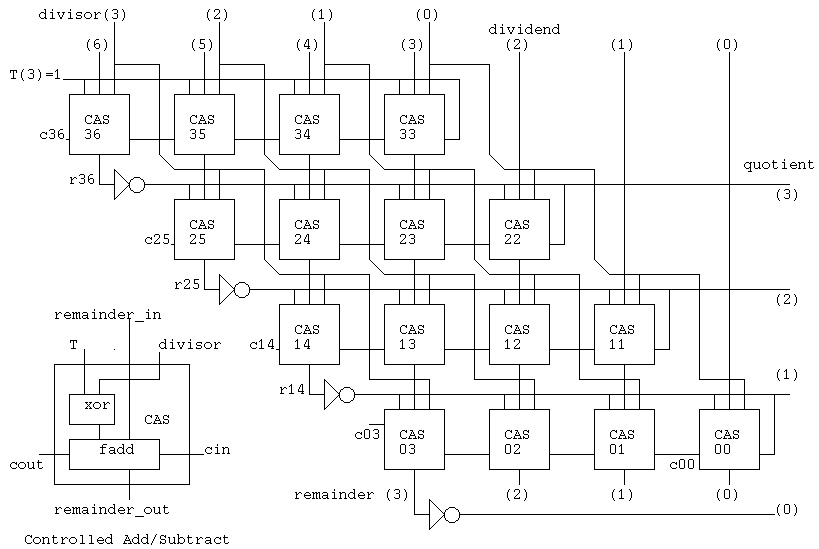
For part1 project you are given divcas16.vhdl
This divides as 32 bit number by a 16 bit number and
produces a 16 bit quotient and 16 bit remainder.
divcas16.vhdl
It would be nice if I could have a 4-bit radix 2 or radix 4 SRT
division schematic here. Parallel circuits that perform division
may use (-2, -1, 0, 1, 2) values for intermediate signals.
Two or more bits of the quotient may be computed at each stage,
based on a table and a few bits of the divisor and partial
remainder.
SRT Divide, click on slide show .pdf
SRT Divide .pdf local
freepatentsonline.com/5272660.html
Software can be copyrighted. Just doing a physical embodiment makes
you the owner of the copyright. Add Copyright year name to the
document or computer file. If you want your copyright to stand up
in a court of law, you need to file the copyright. Get the latest
information, at one time there was a $40.00 filing fee and the
copyright was good for 28 years, renewable for 67 more years, for
a total of 95 years.
There is a "fair use" clause that allows personal use of parts
of a copyrighted document.
Software and hardware and processes may be patented. A utility
patent is good for 20 years, a design patent is good for 14 years.
The cost of completing the process of getting a patent is variable.
20 years ago the average cost was $5,000.00 and today the average
cost is about $15,000.00. There are companies that can help you,
do-it-yourself, with advertised cost starting from about $1,500.00.
(There may be additional maintenance fees at 3 1/2 years etc.)
((It may take a year or more to get a patent.))
One version of the process to get a patent is:
divcas4_test.vhdl
divcas4_test.out
Note that the output includes the time.
Observe the first few lines of printout replacing 'U' undefined,
meaning not computed, with zeros or ones. Unfortunately, if VHDL
prints hexadecimal, any state except one is printed as zero.
For part1 project you are given divcas16.vhdl
This divides as 32 bit number by a 16 bit number and
produces a 16 bit quotient and 16 bit remainder.
divcas16.vhdl
It would be nice if I could have a 4-bit radix 2 or radix 4 SRT
division schematic here. Parallel circuits that perform division
may use (-2, -1, 0, 1, 2) values for intermediate signals.
Two or more bits of the quotient may be computed at each stage,
based on a table and a few bits of the divisor and partial
remainder.
SRT Divide, click on slide show .pdf
SRT Divide .pdf local
freepatentsonline.com/5272660.html
Software can be copyrighted. Just doing a physical embodiment makes
you the owner of the copyright. Add Copyright year name to the
document or computer file. If you want your copyright to stand up
in a court of law, you need to file the copyright. Get the latest
information, at one time there was a $40.00 filing fee and the
copyright was good for 28 years, renewable for 67 more years, for
a total of 95 years.
There is a "fair use" clause that allows personal use of parts
of a copyrighted document.
Software and hardware and processes may be patented. A utility
patent is good for 20 years, a design patent is good for 14 years.
The cost of completing the process of getting a patent is variable.
20 years ago the average cost was $5,000.00 and today the average
cost is about $15,000.00. There are companies that can help you,
do-it-yourself, with advertised cost starting from about $1,500.00.
(There may be additional maintenance fees at 3 1/2 years etc.)
((It may take a year or more to get a patent.))
One version of the process to get a patent is:
 There is no "fair use" clause on patents.
Almost all Numerical Computation arithmetic is performed using
IEEE 754-1985 Standard for Binary Floating-Point Arithmetic.
The two formats that we deal with in practice are the 32 bit and
64 bit formats. You need to know how to get the format you desire
in the language you are programming. Complex numbers use two values.
older
C Java Fortran 95 Fortran Ada 95 MATLAB
------ ------ ---------------- ------- ---------- -------
32 bit float float real real float N/A
64 bit double double double precision real*8 long_float 'default'
complex
32 bit 'none' 'none' complex complex complex N/A
64 bit 'none' 'none' double complex complex*16 long_complex 'default'
'none' means not provided by the language (may be available as a library)
N/A means not available, you get the default.
IEEE Floating-Point numbers are stored as follows:
The single format 32 bit has
1 bit for sign, 8 bits for exponent, 23 bits for fraction
The double format 64 bit has
1 bit for sign, 11 bits for exponent, 52 bits for fraction
There is actually a '1' in the 24th and 53rd bit to the left
of the fraction that is not stored. The fraction including
the non stored bit is called a significand.
The exponent is stored as a biased value, not a signed value.
The 8-bit has 127 added, the 11-bit has 1023 added.
A few values of the exponent are "stolen" for
special values, +/- infinity, not a number, etc.
Floating point numbers are sign magnitude. Invert the sign bit to negate.
Some example numbers and their bit patterns:
decimal
stored hexadecimal sign exponent fraction significand
bit in binary
The "1" is not stored
| biased
31 30....23 22....................0 exponent
1.0
3F 80 00 00 0 01111111 00000000000000000000000 1.0 * 2^(127-127)
0.5
3F 00 00 00 0 01111110 00000000000000000000000 1.0 * 2^(126-127)
0.75
3F 40 00 00 0 01111110 10000000000000000000000 1.1 * 2^(126-127)
0.9999995
3F 7F FF FF 0 01111110 11111111111111111111111 1.1111* 2^(126-127)
0.1
3D CC CC CD 0 01111011 10011001100110011001101 1.1001* 2^(123-127)
63 62...... 52 51 ..... 0
1.0
3F F0 00 00 00 00 00 00 0 01111111111 000 ... 000 1.0 * 2^(1023-1023)
0.5
3F E0 00 00 00 00 00 00 0 01111111110 000 ... 000 1.0 * 2^(1022-1023)
0.75
3F E8 00 00 00 00 00 00 0 01111111110 100 ... 000 1.1 * 2^(1022-1023)
0.9999999999999995
3F EF FF FF FF FF FF FF 0 01111111110 111 ... 1.11111* 2^(1022-1023)
0.1
3F B9 99 99 99 99 99 9A 0 01111111011 10011..1010 1.10011* 2^(1019-1023)
|
sign exponent fraction |
before storing subtract bias
Note that an integer in the range 0 to 2^23 -1 may be represented exactly.
Any power of two in the range -126 to +127 times such an integer may also
be represented exactly. Numbers such as 0.1, 0.3, 1.0/5.0, 1.0/9.0 are
represented approximately. 0.75 is 3/4 which is exact.
Some languages are careful to represent approximated numbers
accurate to plus or minus the least significant bit.
Other languages may be less accurate.
/* flt.c just to look at .o file with hdump */
void flt() /* look at IEEE floating point */
{
float x1 = 1.0f;
float x2 = 0.5f;
float x3 = 0.75f;
float x4 = 0.99999f;
float x5 = 0.1f;
double d1 = 1.0;
double d2 = 0.5;
double d3 = 0.75;
double d4 = 0.99999999; The "1" not stored
double d5 = 0.1; in binary
} |
31 30....23 22....................0 |
3F 80 00 00 0 01111111 00000000000000000000000 1.0 * 2^(127-127)
3F 00 00 00 0 01111110 00000000000000000000000 1.0 * 2^(126-127)
3F 40 00 00 0 01111110 10000000000000000000000 1.1 * 2^(126-127)
3F 7F FF 58 0 01111110 11111111111111101011000 1.1111* 2^(126-127)
3D CC CC CD 0 01111011 10011001100110011001101 1.1001* 2^(123-127)
63 62...... 52 51 ..... 0
3F F0 00 00 00 00 00 00 0 01111111111 000 ... 000 1.0 * 2^(1023-1023)
3F E0 00 00 00 00 00 00 0 01111111110 000 ... 000 1.0 * 2^(1022-1023)
3F E8 00 00 00 00 00 00 0 01111111110 100 ... 000 1.1 * 2^(1022-1023)
3F EF FF FF FA A1 9C 47 0 01111111110 111 ... 1.11111* 2^(1022-1023)
3F B9 99 99 99 99 99 9A 0 01111111011 1001 ..1010 1.10011* 2^(1019-1023)
|
sign exponent fraction |
subtract bias
decimal binary fraction / decimal exponent IEEE normalize
binary
Now, all the above is the memory, RAM, format.
Upon a load operation of either float or double into one of the floating point
registers, the format in the register extended to greater precision
than double. All floating point arithmetic is performed at this
greater precision. Upon a store operation, the greater precision is
reduced to the memory format, possibly with rounding.
From a programming viewpoint, always use double.
exponents must be the same for add and subtract!
A = 3.5 * 10^6 a = 11.1 * 2^6 1.11 * 2^7
B = 2.5 * 10^5 b = 10.1 * 2^5 1.01 * 2^6
A+B 3.50 * 10^6 a+b 11.10 * 2^6 1.110 * 2^7
+ 0.25 * 10^6 + 1.01 * 2^6 + 0.101 * 2^7
_____________ ______________ ------------
3.75 * 10^6 100.11 * 2^6 10.011 * 2^7
normalize 1.0011 * 2^8
IEEE
A-B 3.50 * 10^6
normalize 0.10011 * 2*9
- 0.25 * 10^6 fraction
-------------
3.25 * 10^6
A*B 3.50 * 10^6
* 2.5 * 10^5
-------------
8.75 * 10^11
A/B 3.5 *10^6 / 2.5 *10^5 = 1.4 * 10^1
The mathematical basis for floating point is simple algebra
The common uses are in computer arithmetic and scientific notation
given: a number x1 expressed as 10^e1 * f1
then 10 is the base, e1 is the exponent and f1 is the fraction
example x1 = 10^3 * .1234 means x1 = 123.4 or .1234*10^3
or in computer notation 0.1234E3
In computers the base is chosen to be 2, i.e. binary notation
for x1 = 2^e1 * f1 where e1=3 and f1 = .1011
then x1 = 101.1 base 2 or, converting to decimal x1 = 5.5 base 10
Computers store the sign bit, 1=negative, the exponent and the
fraction in a floating point word that may be 32 or 64 bits.
The operations of add, subtract, multiply and divide are defined as:
Given x1 = 2^e1 * f1
x2 = 2^e2 * f2 and e2 <= e1
x1 + x2 = 2^e1 *(f1 + 2^-(e1-e2) * f2) f2 is shifted then added to f1
x1 - x2 = 2^e1 *(f1 - 2^-(e1-e2) * f2) f2 is shifted then subtracted from f1
x1 * x2 = 2^(e1+e2) * f1 * f2
x1 / x2 = 2^(e1-e2) * (f1 / f2)
an additional operation is usually needed, normalization.
if the resulting "fraction" has digits to the left of the binary
point, then the fraction is shifted right and one is added to
the exponent for each bit shifted until the result is a fraction.
We will use fraction normalization, not IEEE normalization:
if the resulting "fraction" has zeros immediately to the right of
the binary point, then the fraction is shifted left and one is
subtracted from the exponent for each bit shifted until there
is a non zero digit to the right of the binary point.
Numeric examples using equations:
(exponents are decimal integers, fractions are decimal)
(normalized numbers have 1.0 > fraction >= 0.5)
(note fraction strictly less than 1.0, greater than or equal 0.5)
x1 = 2^4 * 0.5 or x1 = 8.0
x2 = 2^2 * 0.5 or x2 = 2.0
x1 + x2 = 2^4 * (.5 + 2^-(4-2) * .5) = 2^4 * (.5 + .125) = 2^4 * .625
x1 - x2 = 2^4 * (.5 - 2^-(4-2) * .5) = 2^4 * (.5 - .125) = 2^4 * .375
not normalized, multiply fraction by 2, subtract 1 from exponent
= 2^3 * .75
x1 * x2 = 2^(4+2) * (.5*.5) = 2^6 * .25 not normalized
= 2^5 * .5 normalized
x1 / x2 = 2^(4-2) * (.5/.5) = 2^2 * 1.0 not normalized
= 2^3 * .5 normalized
Numeric examples, people friendly:
(exponents are decimal integers, fractions are decimal)
(normalized numbers have 1.0 > fraction >= 0.5)
x1 = 0.5 * 2^4
x2 = 0.5 * 2^2
x1 + x2 = 0.500 * 2^4
+ 0.125 * 2^4 unnormalize to make exponents equal
-----------
0.625 * 2^4 result is normalized, done.
x1 - x2 = 0.500 * 2^4
- 0.125 * 2^4 unnormalize to make exponents equal
-----------
0.375 * 2^4 result is not normalized
0.750 * 2^3 double fraction, halve exponential
x1 * x2 = 0.5 * 0.5 * 2^2 * 2^4 = 0.25 * 2^6 not normalized
= 0.5 * 2^5 normalized
x1 / x2 = (.5/.5) * 2^4/2^2 = 1.0 * 2^2 not normalized
= 0.5 * 2^3 normalized
halve fraction, double exponential
IEEE 754 Floating Point Standard
A few minor problems, e.g. the square root of all complex numbers
are in the right half of the complex plane and thus the real
part of the square root should never be negative. As a concession
to early hardware, the standard define the sqrt(-0) to be -0
rather than +0. Several places the standard uses the word should.
If a standard is specifying something, the word shall is typically used.
Basic decisions and operations for floating point add and subtract:
 The decisions indicated above could be used to design the control
component shown in the data path diagram below:
The decisions indicated above could be used to design the control
component shown in the data path diagram below:
 A hint on normalization, using computer scientific notation:
1.0E-8 == 10.0E-9 == 0.01E-6 == 0.00000001 == 10ns == 0.01 microseconds
1.0E8 == 0.1E9 == 100.0E6 == 100,000,000 == 100MHz == 0.1 GHz
1.0/1.0GHz = 1ns clock period
Some graphics boards have large computing capacity and
some are releasing the specs so programmers can use the
computing capacity.
nVidia example 2007
512-core by 2011, more today
Programming 512 cores or more with CUDA or OpenCL is quite a challenge.
New languages are coming, not optimized yet.
Fortunately, CMSC 411 does not require VHDL for floating point,
just the ability to manually do floating point add, subtract,
multiply and divide. (Examples above and in class on board.)
A hint on normalization, using computer scientific notation:
1.0E-8 == 10.0E-9 == 0.01E-6 == 0.00000001 == 10ns == 0.01 microseconds
1.0E8 == 0.1E9 == 100.0E6 == 100,000,000 == 100MHz == 0.1 GHz
1.0/1.0GHz = 1ns clock period
Some graphics boards have large computing capacity and
some are releasing the specs so programmers can use the
computing capacity.
nVidia example 2007
512-core by 2011, more today
Programming 512 cores or more with CUDA or OpenCL is quite a challenge.
New languages are coming, not optimized yet.
Fortunately, CMSC 411 does not require VHDL for floating point,
just the ability to manually do floating point add, subtract,
multiply and divide. (Examples above and in class on board.)
Debugging VHDL (or almost any computer input)
1) Expect errors. Nobody's perfect.
2) Automate to make it easy to re-run, e.g. Makefile_411 or Makefile_ghdl
for HW4, you may use either or both.
make -f Makefile_411 tadd32.out # cadence
diff -iw tadd32.out tadd32.chk
make -f Makefile_ghdl tadd32.gout # GHDL diff in Makefile_ghdl
diff -iw tadd32.gout tadd32.chkg
The .out and .gout differ in extra lines, vhdl output should be the same.
Use Makefile or do a lot of typing: for cadence
run_ncvhdl.bash -v93 -messages -linedebug -cdslib ~/cs411/vhdl2/cds.lib -hdlvar ~/cs411/vhdl2/hdl.var -smartorder add32.vhdl tadd32.vhdl
run_ncelab.bash -v93 -messages -access rwc -cdslib ~/cs411/vhdl2/cds.lib -hdlvar ~/cs411/vhdl2/hdl.var tadd32
run_ncsim.bash -input tadd32.run -batch -logfile tadd32.out -messages -cdslib ~/cs411/vhdl2/cds.lib -hdlvar ~/cs411/vhdl2/hdl.var tadd32
Use Makefile or do a lot of typing: for GHDL
ghdl -a --ieee=synopsys add32.vhdl
ghdl -a --ieee=synopsys tadd32.vhdl
ghdl -e --ieee=synopsys tadd32
ghdl -r --ieee=synopsys tadd32 --stop-time=65ns > tadd32.gout
diff -iw tadd32.gout tadd32.chkg
3) for rest HW6, part1, part2a, part2b, part3a, part3b
HW6
make -f Makefile_411 pmull16_test.out # cadence
diff -iw pmul16_test.out pmul16.chk
make -f Makefile_ghdl tadd32.gout # GHDL
diff -iw pmul16_test.gout pmul16.chkg
part1
make -f Makefile_411 part1.out # cadence
diff -iw part1.out part1.chk
make -f Makefile_ghdl part1.gout # GHDL
diff -iw part1.gout part1.chkg
part2a
make -f Makefile_411 part2a.out # cadence
diff -iw part2a.out part2a.chk
make -f Makefile_ghdl part2a.gout # GHDL
diff -iw part2a.gout part2a.chkg
part2b
make -f Makefile_411 part2b.out # cadence
diff -iw part2b.out part2b.chk
make -f Makefile_ghdl part2b.gout # GHDL
diff -iw part2b.gout part2b.chkg
part3a
make -f Makefile_411 part3a.out # cadence
diff -iw part3a.out part3a.chk
make -f Makefile_ghdl part3a.gout # GHDL
diff -iw part3a.gout part3a.chkg
part3b
make -f Makefile_411 part3b.out # cadence
diff -iw part3b.out part3b.chk
make -f Makefile_ghdl part3b.gout # GHDL
diff -iw part3b.gout part3b.gchk
4) FIX THE FIRST ERROR !!!!
Yes, you can fix other errors also, but one error can cause
a cascading effect and produce many errors.
Don't panic when there was only one error, you fixed that,
then the next run you get 37 errors. The compiler has stages,
it stops on a stage if there is an error. Fixing that error
lets the compiler move to the next stage and check for other
types of errors. Go to step 3)
5) Don't give up. Don't make wild guesses. Do experiment with
one change at a time. You may actually have to read some
of the lectures :)
6) Your circuit compiles and simulates but the output is not
correct. Solution: find first difference, or add debug print.
OK to put in debug printout, remove or comment out before submit.
Most circuits in this course have a print process. You can
easily add printout of more signals. Look for the existing
code that has 'write' and 'writeline' statements.
To print out some signal, xxx, after a 'writeline' statement add
write(my_line, string'(" xxx=")); -- label printout
hwrite(my_line, xxx); -- hex for long signals
write(my_line, string'(" enb="));
write(my_line, enb); -- bit for single values
writeline(output, my_line); -- outputs line
7) You have a signal, xxx, that seems to be wrong and you can not
find when it gets the wrong value. OK, create a new process to
print every change and when it occurs.
prtxxx: process (xxx)
variable my_line : LINE; -- my_line needs to be defined
begin
write(my_line, string'("xxx="));
write(my_line, xxx); -- or hwrite for long signals
write(my_line, string'(" at="));
write(my_line, now); -- "now" is simulation time
writeline(output, my_line); -- outputs line
end process prtxxx;
When adding 'write' statements, you may need to add the
context clause in front of the enclosing design unit. e.g.
library STD;
use STD.textio.all; -- defines LINE, writeline, etc.
library IEEE;
use IEEE.std_logic_1164.all;
use IEEE.std_logic_textio.all; -- defines write on std_logic (_vector)
8) Read your code.
Every identifier must be declared before it is used.
Every signal MUST be set exactly once, e.g.
xxx <= a;
xxx <= b; -- somewhere else, BAD !
-- all hardware runs all the time
-- the ordering of some statements does not matter
a0: fadd port map(a(0), b(0), cin , sum(0), c(0));
a1: fadd port map(a(1), b(1), c(0), sum(1), c(0));
#### BAD !
Signals must match in type and size. An error having
"shape mismatch" means incompatible size. You can not put
one bit into a 32 bit signal nor 32 bits into a one bit signal.
"...type... error" Are you putting an integer into a std_logic?
You can not put an identifier of type std_logic into
std_logic_vector. a(31 downto 28) is of type std_logic_vector,
a(31) is of type std_logic.
Everywhere a specific signal name is used, these points are
wired together. For VHDL simulation purposes, all points on a
wire always have exactly the same value. Zero propagation delay
through a wire. Be careful what you wire together. Use the VHDL
reserved word 'open' for open circuits rather than NC for
no connection.
 ncsim: 05.40-s011: (c) Copyright 1995-2005 Cadence Design Systems, Inc.
ncsim> run 7 ns
A= 1 B= 1 C= U D= U CNC= U DNC= U NC= U at time 0 ns
A= 1 B= 1 C= U D= U CNC= U DNC= U NC= U at time 1 ns
A= 1 B= 1 C= 1 D= U CNC= U DNC= U NC= U at time 2 ns
A= 1 B= 1 C= 1 D= U CNC= U DNC= U NC= U at time 3 ns
A= 1 B= 1 C= 1 D= 1 CNC= U DNC= U NC= U at time 4 ns
A= 1 B= 1 C= 1 D= 1 CNC= U DNC= U NC= U at time 5 ns
A= 1 B= 1 C= 1 D= 1 CNC= U DNC= U NC= U at time 6 ns
Ran until 7 NS + 0
ncsim> exit
!!! !!! never set due to connection
-- use_open.vhdl
library IEEE;
use IEEE.std_logic_1164.all;
entity AN is
port(IN1 : in std_logic;
IN2 : in std_logic;
OUTB : inout std_logic; -- because used internally, bad design
OUTT : out std_logic);
end entity AN;
architecture circuits of AN is
begin -- circuits
OUTB <= IN1 nand IN2 after 1 ns;
OUTT <= not OUTB after 1 ns;
end architecture circuits; -- of AN
library IEEE;
use IEEE.std_logic_1164.all;
use STD.textio.all;
use IEEE.std_logic_textio.all;
entity use_open is
end entity use_open;
architecture circuits of use_open is
signal A : std_logic := '1';
signal B : std_logic := '1';
signal C, CNC : std_logic;
signal D, DNC : std_logic;
signal NC : std_logic := '1'; -- for no connection or tied off
begin
my_print : process is
variable my_line : line;
begin
write(my_line, string'("A= "));
write(my_line, A);
write(my_line, string'(" B= "));
write(my_line, B);
write(my_line, string'(" C= "));
write(my_line, C);
write(my_line, string'(" D= "));
write(my_line, D);
write(my_line, string'(" CNC= "));
write(my_line, CNC);
write(my_line, string'(" DNC= "));
write(my_line, DNC);
write(my_line, string'(" NC= "));
write(my_line, NC);
write(my_line, string'(" at time "));
write(my_line, now);
writeline(output, my_line);
wait for 1 ns;
end process my_print;
n01: entity WORK.AN port map(A, B, open, C);
n02: entity WORK.AN port map('1', C, open, D);
n03: entity WORK.AN port map(A, B, NC, CNC);
n04: entity WORK.AN port map('1', CNC, NC, DNC);
end architecture circuits; -- of use_open
Truth tables using type std_logic
t_table.vhdl
Now, some Cadence VHDL error messages.
-- error.vhdl demonstrate VHDL compiler error messages
library IEEE;
use IEEE.std_logic_1164.all;
entity AN is
port(IN1 : in std_logic;
IN2 : in std_logic;
OUTB : inout std_logic; -- because used internally
OUTT : out std_logic;);
end entity AN;
architecture circuits of AN is
signal aaa : std_logic;
begin -- circuits
OUTB <= aa and IN1 and IN2 after 1 ns;
OUTT <= not OUTB after 1 ns;
end architecture circuits; -- of AN
old output:
ncvhdl: 05.40-s011: (c) Copyright 1995-2005 Cadence Design Systems, Inc.
OUTT : out std_logic;);
|
ncvhdl_p: *E,PORNKW (error.vhdl,10|28): identifier expected.
OUTT : out std_logic;);
|
ncvhdl_p: *E,MISCOL (error.vhdl,10|28): expecting a colon (':') 87[4.3.3] 93[4.3.2].
OUTT : out std_logic;);
|
ncvhdl_p: *E,PORNKW (error.vhdl,10|31): identifier expected.
OUTT : out std_logic;);
|
ncvhdl_p: *E,MISCOL (error.vhdl,10|31): expecting a colon (':') 87[4.3.3] 93[4.3.2].
end entity AN;
|
ncvhdl_p: *E,EXPRIS (error.vhdl,11|13): expecting the reserved word 'IS' [1.1].
OUTB <= aa and IN1 and IN2 after 1 ns;
|
ncvhdl_p: *E,IDENTU (error.vhdl,16|11): identifier (AA) is not declared [10.3].
Now you are ready to tackle Homework 6
To simplify
ncsim: 05.40-s011: (c) Copyright 1995-2005 Cadence Design Systems, Inc.
ncsim> run 7 ns
A= 1 B= 1 C= U D= U CNC= U DNC= U NC= U at time 0 ns
A= 1 B= 1 C= U D= U CNC= U DNC= U NC= U at time 1 ns
A= 1 B= 1 C= 1 D= U CNC= U DNC= U NC= U at time 2 ns
A= 1 B= 1 C= 1 D= U CNC= U DNC= U NC= U at time 3 ns
A= 1 B= 1 C= 1 D= 1 CNC= U DNC= U NC= U at time 4 ns
A= 1 B= 1 C= 1 D= 1 CNC= U DNC= U NC= U at time 5 ns
A= 1 B= 1 C= 1 D= 1 CNC= U DNC= U NC= U at time 6 ns
Ran until 7 NS + 0
ncsim> exit
!!! !!! never set due to connection
-- use_open.vhdl
library IEEE;
use IEEE.std_logic_1164.all;
entity AN is
port(IN1 : in std_logic;
IN2 : in std_logic;
OUTB : inout std_logic; -- because used internally, bad design
OUTT : out std_logic);
end entity AN;
architecture circuits of AN is
begin -- circuits
OUTB <= IN1 nand IN2 after 1 ns;
OUTT <= not OUTB after 1 ns;
end architecture circuits; -- of AN
library IEEE;
use IEEE.std_logic_1164.all;
use STD.textio.all;
use IEEE.std_logic_textio.all;
entity use_open is
end entity use_open;
architecture circuits of use_open is
signal A : std_logic := '1';
signal B : std_logic := '1';
signal C, CNC : std_logic;
signal D, DNC : std_logic;
signal NC : std_logic := '1'; -- for no connection or tied off
begin
my_print : process is
variable my_line : line;
begin
write(my_line, string'("A= "));
write(my_line, A);
write(my_line, string'(" B= "));
write(my_line, B);
write(my_line, string'(" C= "));
write(my_line, C);
write(my_line, string'(" D= "));
write(my_line, D);
write(my_line, string'(" CNC= "));
write(my_line, CNC);
write(my_line, string'(" DNC= "));
write(my_line, DNC);
write(my_line, string'(" NC= "));
write(my_line, NC);
write(my_line, string'(" at time "));
write(my_line, now);
writeline(output, my_line);
wait for 1 ns;
end process my_print;
n01: entity WORK.AN port map(A, B, open, C);
n02: entity WORK.AN port map('1', C, open, D);
n03: entity WORK.AN port map(A, B, NC, CNC);
n04: entity WORK.AN port map('1', CNC, NC, DNC);
end architecture circuits; -- of use_open
Truth tables using type std_logic
t_table.vhdl
Now, some Cadence VHDL error messages.
-- error.vhdl demonstrate VHDL compiler error messages
library IEEE;
use IEEE.std_logic_1164.all;
entity AN is
port(IN1 : in std_logic;
IN2 : in std_logic;
OUTB : inout std_logic; -- because used internally
OUTT : out std_logic;);
end entity AN;
architecture circuits of AN is
signal aaa : std_logic;
begin -- circuits
OUTB <= aa and IN1 and IN2 after 1 ns;
OUTT <= not OUTB after 1 ns;
end architecture circuits; -- of AN
old output:
ncvhdl: 05.40-s011: (c) Copyright 1995-2005 Cadence Design Systems, Inc.
OUTT : out std_logic;);
|
ncvhdl_p: *E,PORNKW (error.vhdl,10|28): identifier expected.
OUTT : out std_logic;);
|
ncvhdl_p: *E,MISCOL (error.vhdl,10|28): expecting a colon (':') 87[4.3.3] 93[4.3.2].
OUTT : out std_logic;);
|
ncvhdl_p: *E,PORNKW (error.vhdl,10|31): identifier expected.
OUTT : out std_logic;);
|
ncvhdl_p: *E,MISCOL (error.vhdl,10|31): expecting a colon (':') 87[4.3.3] 93[4.3.2].
end entity AN;
|
ncvhdl_p: *E,EXPRIS (error.vhdl,11|13): expecting the reserved word 'IS' [1.1].
OUTB <= aa and IN1 and IN2 after 1 ns;
|
ncvhdl_p: *E,IDENTU (error.vhdl,16|11): identifier (AA) is not declared [10.3].
Now you are ready to tackle Homework 6
To simplify
 sqrt examples of simplify
Review is paper handout. (not for online classes, open web) Following, microcontrollers, microprogramming and 64-bit. A microcontroller may be a very small and inexpensive device. The basic parts are Combinational Logic, logic gates, and some type of storage, Sequential Logic.For students who have taken CMSC 451, this is the classic Deterministic Automata, a Finite State Machine. A microcontroller may have Read Only Memory, ROM, that contains a microprogram to run the microcontroller. Micro assemblers and micro compilers may be used to generate the microprogram. The microprogram is manufactured in the microcontroller. Micro instructions may be very long, 40 to 64 bits is common. Often there are bits to directly control multiplexors. Often there are groups of bits to directly control other units such as the ALU. There may be bits that go directly to outputs. Every microinstruction may have a jump address. The jump may be a conditional branch based on some state bits.
From Wikipedia wiki/Microcode Terminology: Combinational Logic is just gates. No storage. Sequential Logic has storage, flipflop(s) or register(s). A flipflop or register holds the output until changed. A flipflop or register will have a clock and data will only be input to change state on a clock edge. There may be a clear or set input that does not need a clock signal, typically used to initialize a logic circuit to a known state. This lecture also covers 64-bit machines (If not covered earlier) A 64-bit architecture, by definition, has 64-bit integer registers. Many computers have had 64-bit IEEE floating point for many years. The 64-bit machines have been around for a while as the Alpha and PowerPC yet have become popular for the desktop with the Intel and AMD 64-bit machines.
review for midterm, handout
  open book, open note, download, edit, submit
  OK to scp to windows and use Microsoft Word, scp back, submit.
  OK to use  libreoffice  on gl.umbc.edu  and submit
  Edit by placing  X  after  a)  b)  c) ...
  Also OK to highlight answer.
  Only one answer per question!

  Students with email user name starting  a b c d e f g h i
  download and edit  midterm33a.doc
  download midterm33a.doc


  Students with email user name starting  j k l m n o p q
  download and edit  midterm33b.doc
  download midterm33b.doc


  Students with email user name starting  r s t u v w x y z
  download and edit  midterm33c.doc
  download midterm33c.doc

  Follow instructions in exam, edit, then
  submit  cs411  midterm  midterm33?.doc

  You can do the exam on linux.gl.umbc.edu in your directory
  using libreoffice midterm33?.doc

  cp /afs/umbc.edu/users/s/q/squire/pub/download/midterm33?.doc .
  libreoffice midterm33?.doc
  submit cs411 midterm midterm33?.doc
  rm midterm33?.doc  only if over quota


  Before Exam:
  Review HW2, HW3, HW4 (VHDL) and HW5
  Review WEB Lecture Notes 1 through 13.

  There are  10  types of people:
    Those who know binary.
    Those who do not know binary.

  Teach your children to count in the computer age:
    zero
    one
    two
    three
    four

  Computer bits are numbered from the bottom

    0  0  1  0  1  = 5
    4  3  2  1  0    bit numbers (actually powers of 2)
Last update 9/9/2020
We now start the second half of the semester, focusing on the five part project to simulate part of a real computer. Note that the hardware does not change. Only multiplexer control signals are needed to execute various instructions. The first complete computer architecture is a single cycle design. On each clock cycle this computer executes one instruction. CPI=1 (The clock would be slow compared to pipeline computers in the next lecture.) Signals are inputs to components on the left and outputs of components on the right. Wide lines are 32-bits. Narrow signals are one-bit unless otherwise indicated.Every clock, we use the rising edge, the program counter register, PC, takes the 32 bit input from the left most signal on the diagram. The output of the PC is a memory address for an instruction. The 32 bit instruction is "decoded" by routing various parts of the instruction to various places. Bits 31 downto 26 of the instruction go to the control unit. (The schematic of the control unit is shown below.) Bits 10 downto 0 of the instruction go to the ALU, the shift count and the ALU op code. Bits 25 downto 21 are a register address that is read and the 32 bit contents of that register are placed on read data 1. Bits 20 downto 16 are a register address that is read and the 32 bit contents of that register are placed on read data 2. Bits 15 downto 11 are a register address that may be written with the 32 bit write data. Bits 25 downto 0 go to the jump address computation. The sequence of diagrams that follow will show the control signals and the data paths for various instructions. The bit patterns for our CMSC 411 machine are cs411_opcodes.txt inside the ALU entity The first instruction is the nop instruction. This instruction shows the basic updating of the PC, while changing no other registers or memory. All other instructions shown below, except branch and jump , use this updating of the PC.
nop
The PC plus 4 is the next sequential instruction address. The 32 bit instruction has four bytes. The bottom two bits of all instruction addresses are zero. The instructions are "aligned." The critical control signals are: jump 0 branch 0 MemWrite 0 RegWrite 0 The other control signals are shown for completeness. The next instruction, jump, is just slightly more complex than nop. The bit pattern for jump in cs411_opcodes.txt
jump
Note the wiring where instruction bits 25 downto 0 are shifter left two places. This provides a larger jump range and aligns the address on a quad byte boundary. The top four bits come from the incremented PC and the resulting 32 bit address is routed through the multiplexer back to the PC, ready for the next clock. The critical control signals are: jump 1 MemWrite 0 RegWrite 0 The other control signals are shown for completeness. The next instruction, branch , uses the remainder of the upper schematic to compute a new instruction address relative to the incremented PC. Note that the assembler subtracts 4 from the branch address before generating the machine instruction. The bit pattern for beq in cs411_opcodes.txt
branch
Note the equal comparator immediately next to the registers. This is the design we will use in the project because it provides better performance in the pipeline architecture. If the branch condition is not satisfied, the instruction becomes a nop . The branch condition for beq is that the contents of the registers are the same and a beq instruction is executing. Note the and gate driving the multiplexer. The critical control signals are: jump 0 branch 1 and the equal comparison MemWrite 0 RegWrite 0 The other control signals are shown for completeness. The add instruction is shown with just the data paths and control paths for the instruction shown. The upper control to increment the PC is the same as shown for the nop instruction. The bit pattern for add in cs411_opcodes.txt
add
The contents of two registers are combined in the ALU. The ALU op code in the instruction bits 5 downto 0 would have 100000 for add . Other instructions such as subtract, shift, and, etc follow the same data paths and control, executing the instruction coded in the instruction bits 5 downto 0. The output of the ALU is routed back to the registers and written on the falling edge of the clock, clk. The critical control signals are: jump 0 branch 0 MemtoReg 0 MemWrite 0 Aluop 1 ALUSrc 0 RegWrite 1 RegDst 1 The other control signals are shown for completeness. The load word, lw , instruction computes a memory address using the twos complement offset in the instruction bits 15 downto 0, sign extended to 32 bits and added to a register. The memory is read and the contents from memory is routed through the multiplexer into the destination register. The PC is incremented as shown in the nop instruction. The bit pattern for lw in cs411_opcodes.txt
load word, lw
The critical control signals are: jump 0 branch 0 MemtoReg 1 MemRead 1 MemWrite 0 Aluop 0 the ALU performs an add when Aluop is zero ALUSrc 1 RegWrite 1 RegDst 0 The other control signals are shown for completeness. The store word, sw , instruction computes a memory address using the twos complement offset in the instruction bits 15 downto 0, sign extended to 32 bits and added to a register. The read data 2 is stored in memory. The PC is incremented as shown in the nop instruction. The bit pattern for sw in cs411_opcodes.txt
store word, sw
Note the data path around the ALU into the write data input to the memory The critical control signals are: jump 0 branch 0 MemRead 0 MemWrite 1 Aluop 0 the ALU performs an add when Aluop is zero ALUSrc 1 RegWrite 0 The other control signals are shown for completeness. The add immediate, addi , instruction adds the twos complement bits 15 downto 0 of the instruction to a register and places the sum into the destination register. The PC is incremented as shown in the nop instruction. The bit pattern for addi in cs411_opcodes.txt
add immediate, addi
The critical control signals are: jump 0 branch 0 MemtoReg 0 MemWrite 0 Aluop 0 the ALU performs an add when Aluop is zero ALUSrc 1 RegWrite 1 RegDst 0 The other control signals are shown for completeness. The control schematic for some specific instructions, possibly not this semester, for the one cycle architecture, is:
The shift left 2 circuit is just bent wires. The VHDL is output <= input(29 downto 0) & "00";
The sign extend circuit is just wiring. The input is a 16 bit twos complement word and outputs a 32 bit twos complement word. The VHDL is output(15 downto 0) <= input; output(31 downto 16) <= (others => input(15));
cs411_opcodes.txt different from Computer Organization and Design 1/8/2020 rd is register destination, the result, general register 1 through 31 rs is the first register, A, source, general register 0 through 31 rt is the second register, B, source, general register 0 through 31 --val---- generally a 16 bit number that gets sign extended --adr---- a 16 bit address, gets sign extended and added to (rx) "i" is generally immediate, operand value is in the instruction Opcode Operands Machine code format 6 5 5 5 5 6 number of bits in field 3 3 2 2 2 2 2 2 2 2 2 2 1 1 1 1 1 1 1 1 1 1 1 0 9 8 7 6 5 4 3 2 1 0 9 8 7 6 5 4 3 2 1 0 9 8 7 6 5 4 3 2 1 0 | | | | | 0 0 0 0 0 0 0 0 0 0 0 0 0 0 0 0 0 0 0 0 0 0 0 0 0 0 0 0 0 0 0 0 nop 0 0 0 0 0 0 a a a a a b b b b b r r r r r -ignored- 1 0 0 0 0 0 add r,a,b 0 0 0 0 0 0 a a a a a b b b b b r r r r r -ignored- 1 0 0 0 1 0 sub r,a,b 0 0 0 0 0 0 a a a a a b b b b b r r r r r -ignored- 0 1 1 0 0 0 mul r,a,b 0 0 0 0 0 0 a a a a a b b b b b r r r r r -ignored- 0 1 1 0 1 1 div r,a,b 0 0 0 0 0 0 a a a a a b b b b b r r r r r -ignored- 0 0 1 1 0 1 and r,a,b 0 0 0 0 0 0 a a a a a b b b b b r r r r r -ignored- 0 0 1 1 1 1 or r,a,b 0 0 0 0 0 0 0 0 0 0 0 b b b b b r r r r r s s s s s 0 0 0 0 1 1 srl r,b,s 0 0 0 0 0 0 0 0 0 0 0 b b b b b r r r r r s s s s s 0 0 0 0 1 0 sll r,b,s 0 0 0 0 0 0 0 0 0 0 0 b b b b b r r r r r -ignored- 0 0 1 0 1 1 cmpl r,b 0 0 0 0 1 0 -----address to bits (27:2) of PC------------------ j adr 0 0 1 1 1 1 x x x x x r r r r r ---2's complement value-------- lwim r,val(x) 0 0 1 1 0 0 x x x x x r r r r r ---2's complement value-------- addi r,val(x) 0 1 1 1 0 1 a a a a a b b b b b ---2's complement address------ beq a,b,adr 1 0 0 0 1 1 x x x x x r r r r r ---2's complement address------ lw r,adr(x) 1 0 1 0 1 1 x x x x x b b b b b ---2's complement address------ sw b,adr(x) Definitions: nop no operation, no programmer visible registers or memory are changed, except PC <= PC+4 j adr bits 0 through 25 of the instruction are inserted into PC(27:2) probably should zero bits PC(1:0) but should be zero already lw r,adr(x) load word into register r from memory location (register x plus sign extended adr field) sw b,adr(x) store word from register b into memory location (register x plus sign extended adr field) beq a,b,adr branch on equal, if the contents of register a are equal to the contents of register b, add the, shifted by two, sign extended adr to the PC (The PC will have 4 added by then) lwim r,val(x) add immediate, the contents of register x is added to the sign extended value and the result put into register r addi r,val(x) add immediate, the contents of register x is added to the sign extended value and the result is added to register r add r,a,b add register a to register b and put result into register r sub r,a,b subtract register b from register a and put result into register r mul r,a,b multiply register a by register b and put result into register r div r,a,b divide register a by register b and put result into register r and r,a,b and register a to register b and put result into register r or r,a,b or register a to register b and put result into register r srl r,b,s shift the contents of register b by s places right and put result in register r sll r,b,s shift the contents of register b by s places left and put result in register r cmpl r,b one's complement of register b goes into register r Also: no instructions are to have side effects or additional "features" last updated 1/8/2020 (slight difference in opcodes from previous semesters)
First, a few definitions:
Pipelining : Multiple instructions being executed, each in a different
stage of their execution. A form of parallelism.
Super Pipelining : Advertising term, just longer pipelines.
Super Scalar : Having multiple ALU's. There may be a mix of some
integer ALU's and some Floating Point ALU's.
Multiple Issue : Starting a few instructions every clock.
The CPI can be a fraction, 4 issue gives a CPI of 1/4 .
Dynamic Pipeline : This may include all of the above and also can
reorder instructions, use data forwarding and
hazard workarounds.
Pipeline Stages : For our study of the MIPS architecture,
IF Instruction Fetch stage
ID Instruction Decode stage
EX Execute stage
MEM Memory access stage
WB Write Back into register stage
Hyper anything : Generally advertising terminology.
Consider the single cycle machine in the previous lecture.
The goal is to speed up the execution of programs, long sequences
of instructions. Keeping the same manufacturing technology, we can
look at speeding up the clock by inserting clocked registers at
key points. Note the placement of blue registers that tries to
minimize the gate delay time between any pair of registers.
Thus, allowing a faster clock.
 This is called approximate because some additional design must
be performed, mostly on "control", that must now be distributed.
The next step in the design, for our project, is to pass the
instruction along the pipeline and keep the design of each
stage of the pipeline simple, just driven by the instruction
presently in that stage.
This is called approximate because some additional design must
be performed, mostly on "control", that must now be distributed.
The next step in the design, for our project, is to pass the
instruction along the pipeline and keep the design of each
stage of the pipeline simple, just driven by the instruction
presently in that stage.
 pipe1.vhdl implementation moves instruction
note clock and reset generation
look at register behavioral implementation
instruction memory is preloaded
pipe1.out just numbers used for demonstration
pipe1.vhdl implementation moves instruction
note clock and reset generation
look at register behavioral implementation
instruction memory is preloaded
pipe1.out just numbers used for demonstration
Pipelined Architecture with distributed control
 pipe2.vhdl note additional entities
equal6 for easy decoding
data memory behavioral implementation
pipe2.out instructions move through stages
pipe2.vhdl note additional entities
equal6 for easy decoding
data memory behavioral implementation
pipe2.out instructions move through stages
Timing analysis
Consider four instructions being executed.
First on the single cycle architecture, needing 8ns per instruction.
The time for each part of the circuit is shown.
The clock would be:
+---------------+ +---------------+ +------
| | | | |
-+ +---------------+ +---------------+
Single cycle execution 125MHZ clock
0 1 2 3 4 5 6 7 8 9 10 11 12 13 14 15 16 17ns
| | | | | | | | | | | | | | | | | |
+-------+---+-------+-------+---+
|IF |ID | EX | MEM |WB |
+-------+---+-------+-------+---+
+-------+---+-------+-------+---+
|IF |ID | EX | MEM |WB |
+-------+---+-------+-------+---+
+---
|IF ... 24ns
+---
... 32ns
The four instructions finished in 32ns.
An instruction started every 8ns.
An instruction finished every 8ns.
Now, the pipelined architecture has the clock determined by the slowest
part between clocked registers. Typically, the ALU. Thus use the same
ALU time as above, the clock would be:
+---+ +---+ +---+ +---+ +---+ +---+ +---+ +---+ +---+
| | | | | | | | | | | | | | | | | |
-+ +---+ +---+ +---+ +---+ +---+ +---+ +---+ +---+ +-
Pipelined Execution 500MHZ clock **
+-------+-------+-------+-------+-------+
|IF |ID reg| EX | MEM |reg WB |
+-------+-------+-------+-------+-------+
+-------+-------+-------+-------+-------+
|IF |ID reg| EX | MEM |reg WB |
+-------+-------+-------+-------+-------+
+-------+-------+-------+-------+-------+
|IF |ID reg| EX | MEM |reg WB |
+-------+-------+-------+-------+-------+
+-------+-------+-------+-------+-------+
|IF |ID reg| EX | MEM |reg WB |
+-------+-------+-------+-------+-------+
**
| | | | | | | | | | | | | | | | | |
0 1 2 3 4 5 6 7 8 9 10 11 12 13 14 15 16 17ns
The four instructions finished in 16ns. (But, the speedup is not 2)
An instruction started every 2ns.
An instruction finished every 2ns. Thus, the speedup is 8ns/2ns = 4 .
Since an instruction finishes every 2ns for the pipelined architecture and
every 8ns for the single cycle architecture, the speedup will be
8ns/2ns = 4. The speedup would change with various numbers of instructions
if the total time was used. Thus, the time between the start or end of
adjacent instructions is used in computing speedup.
Note the ** above in the pipeline. The first of the four instructions
may load a value in a register. This load takes place on the falling
edge of the clock. The fourth instruction is the earliest instruction
that could use the register loaded by the first instruction. The
use of the register comes after the rising edge of the clock. Thus use
of both halves of the clock cycle is important to this architecture and
to many modern computer architectures.
Remember, every stage of the pipeline must be the same time duration.
The system clock is used by all pipeline registers.
The slowest stage determines this time duration and thus determines
the maximum clock frequency.
The worse case delay that does not happen often because of optimizing
compilers, is a load word, lw, instruction followed by an instruction
that needs the value just loaded. The sequence of instructions, for
this unoptimized architecture, would be:
lw $1,val($0) load the 32 bit value at location val into register 1
nop
nop
addi $2,21($1) register 1 is available, add 21 and put result into reg 2
As can be seen in the pipelined timing below, lw would load register 1
by 9ns and register 1 would be used by addi by 10ns (**). The actual
add would be finished by 12 ns and register 2 updated sum by 15 ns (***).
+-------+-------+-------+-------+-------+
lw $1,val($0)|IF |ID reg| EX | MEM |reg WB |
+-------+-------+-------+-------+-------+
+-------+-------+-------+-------+-------+
nop |IF |ID reg| EX | MEM |reg WB |
+-------+-------+-------+-------+-------+
+-------+-------+-------+-------+-------+
nop |IF |ID reg| EX | MEM |reg WB |
+-------+-------+-------+-------+-------+
+-------+-------+-------+-------+-------+
addi $2,21($1) |IF |ID reg| EX | MEM |reg WB |
+-------+-------+-------+-------+-------+
** ***
| | | | | | | | | | | | | | | | |
0 1 2 3 4 5 6 7 8 9 10 11 12 13 14 15 16
ns
It is interesting to note some similarity to an IBM Power PC that came
a few years after the MIPS R3000 architecture that is similar to the
above design.
IBM Power PC stages and clock usage
new IBM Power PC
Shipped 2012 at 5.5Ghz
The pipeline for this course with branch and jump optimized:
project part2a adds data forwarding
project part2b adds stall
project part3a adds cache for instructions
project part3b adds cache for data
 Note the three input mux replacing two mux in previous lecture.
Note the distributed control using the equal6 entity:
eq6j: entity WORK.equal6 port map(ID_IR(31 downto 26), "000010", jump);
jumpaddr <= PCP(31 downto 28) & ID_IR(25 downto 0) & "00";
cs411_opcodes.txt look at jump
In a later lecture, we will cover data forwarding to avoid nop's in
arithmetic and automatic stall to avoid putting all nop's in source code.
For the basic machine above, we have the timing shown here.
The branch slot, programming to avoid delays (filling in nop's):
Note: beq and jump always execute the next physical instruction.
This is called the "delayed branch slot", important for HW7.
if(a==b) x=3; /* simple C code */
else x=4;
y=5;
lw $1,a # possible unoptimized assembly language
lw $2,b # no ($0) shown on memory access
nop # wait for b to get into register 2
nop # wait for b to get into register 2
beq $1,$2,lab1
nop # branch slot, always executed *********
addi $1,4 # else part
nop # wait for 4 to get into register 1
nop # wait for 4 to get into register 1
sw $1,x # x=4;
j lab2
nop # branch slot, always executed *********
lab1: addi $1,3 # true part
nop # wait for 3 to get into register 1
nop # wait for 3 to get into register 1
sw $1,x # x=3;
lab2: addi $1,5 # after if-else, always execute
nop # wait for 5 to get into register 1
nop # wait for 5 to get into register 1
sw $1,y # y=5;
Unoptimized, 20 instructions. This code needed for project part1
Now, a smart compiler would produce the optimized code:
lw $1,a # possible unoptimized assembly language
lw $2,b # no ($0) shown on memory access
addi $4,4 # for else part later
addi $3,3 # for true part later
beq $1,$2,lab1
addi $5,5 # branch slot, always executed, for after if-else
j lab2
sw $4,x # x=4; in branch slot, always executed !! after jump
lab1: sw $3,x # x=3;
lab2: sw $5,y # y=5;
Optimized, 10 instructions. This code needed for project part2b
The pipeline stage diagram for a==b true is:
1 2 3 4 5 6 7 8 9 10 11 12 clock
lw $1,a IF ID EX MM WB
lw $2,b IF ID EX MM WB
addi $4,4 IF ID EX MM WB
addi $3,3 IF ID EX MM WB
beq $1,$2,L1 IF ID EX MM WB assume equal, branch to L1
addi $5,5 IF ID EX MM WB delayed branch slot
j L2
sw $4,x
L1:sw $3,x IF ID EX MM WB
L2:sw $5,y IF ID EX MM WB
1 2 3 4 5 6 7 8 9 10 11 12
The pipeline stage diagram for a==b false is:
1 2 3 4 5 6 7 8 9 10 11 12 13 clock
lw $1,a IF ID EX MM WB
lw $2,b IF ID EX MM WB
addi $4,4 IF ID EX MM WB
addi $3,3 IF ID EX MM WB
beq $1,$2,L1 IF ID EX MM WB assume not equal
addi $5,5 IF ID EX MM WB
j L2 IF ID EX MM WB jumps to L2
sw $4,x IF ID EX MM WB
L1:sw $3,x
L2:sw $5,y IF ID EX MM WB
1 2 3 4 5 6 7 8 9 10 11 12 13
if(a==b) x=3; /* simple C code */
else x=4;
y=5;
Renaming when there are extra registers that the programmer can
not assess (diagram in Alpha below) with multiple units there can be
multiple issue (parallel execution of instructions)
The architecture sees the binary instructions from the following:
lw $1,a
lw $2,b
nop
sll $3,$1,8
sll $6,$2,8
add $9,$1,$2
sw $3,c
sw $6,d
sw $9,e
lw $1,aa
lw $2,bb
nop
sll $3,$1,8
sll $6,$2,8
add $9,$1,$2
sw $3,cc
sw $6,dd
sw $9,ee
Two ALU's, each with their own pipelines, multiple issue, register renaming:
The architecture executes two instruction streams in parallel.
(Assume only 32 user programmable registers, 80 registers in hardware.)
lw $1,a lw $41,aa
lw $2,b lw $42,bb
nop nop
sll $3,$1,8 sll $43,$41,8
sll $6,$2,8 sll $46,$42,8
add $9,$1,$2 add $49,$41,$42
sw $3,c sw $43,cc
sw $6,d sw $46,dd
sw $9,e sw $49,ee
Out of order execution to avoid delays. As seen in the first example,
changing the order of execution without changing the semantics of the
program can achieve faster execution.
There can be multiple issue when there are multiple arithmetic and
other units. This will require significant hardware to detect the
amount of out of order instructions that can be issued each clock.
Now, hardware can also be pipelined, for example a parallel multiplier.
Suppose we need to have at most 8 gate delays between pipeline
registers.
Note the three input mux replacing two mux in previous lecture.
Note the distributed control using the equal6 entity:
eq6j: entity WORK.equal6 port map(ID_IR(31 downto 26), "000010", jump);
jumpaddr <= PCP(31 downto 28) & ID_IR(25 downto 0) & "00";
cs411_opcodes.txt look at jump
In a later lecture, we will cover data forwarding to avoid nop's in
arithmetic and automatic stall to avoid putting all nop's in source code.
For the basic machine above, we have the timing shown here.
The branch slot, programming to avoid delays (filling in nop's):
Note: beq and jump always execute the next physical instruction.
This is called the "delayed branch slot", important for HW7.
if(a==b) x=3; /* simple C code */
else x=4;
y=5;
lw $1,a # possible unoptimized assembly language
lw $2,b # no ($0) shown on memory access
nop # wait for b to get into register 2
nop # wait for b to get into register 2
beq $1,$2,lab1
nop # branch slot, always executed *********
addi $1,4 # else part
nop # wait for 4 to get into register 1
nop # wait for 4 to get into register 1
sw $1,x # x=4;
j lab2
nop # branch slot, always executed *********
lab1: addi $1,3 # true part
nop # wait for 3 to get into register 1
nop # wait for 3 to get into register 1
sw $1,x # x=3;
lab2: addi $1,5 # after if-else, always execute
nop # wait for 5 to get into register 1
nop # wait for 5 to get into register 1
sw $1,y # y=5;
Unoptimized, 20 instructions. This code needed for project part1
Now, a smart compiler would produce the optimized code:
lw $1,a # possible unoptimized assembly language
lw $2,b # no ($0) shown on memory access
addi $4,4 # for else part later
addi $3,3 # for true part later
beq $1,$2,lab1
addi $5,5 # branch slot, always executed, for after if-else
j lab2
sw $4,x # x=4; in branch slot, always executed !! after jump
lab1: sw $3,x # x=3;
lab2: sw $5,y # y=5;
Optimized, 10 instructions. This code needed for project part2b
The pipeline stage diagram for a==b true is:
1 2 3 4 5 6 7 8 9 10 11 12 clock
lw $1,a IF ID EX MM WB
lw $2,b IF ID EX MM WB
addi $4,4 IF ID EX MM WB
addi $3,3 IF ID EX MM WB
beq $1,$2,L1 IF ID EX MM WB assume equal, branch to L1
addi $5,5 IF ID EX MM WB delayed branch slot
j L2
sw $4,x
L1:sw $3,x IF ID EX MM WB
L2:sw $5,y IF ID EX MM WB
1 2 3 4 5 6 7 8 9 10 11 12
The pipeline stage diagram for a==b false is:
1 2 3 4 5 6 7 8 9 10 11 12 13 clock
lw $1,a IF ID EX MM WB
lw $2,b IF ID EX MM WB
addi $4,4 IF ID EX MM WB
addi $3,3 IF ID EX MM WB
beq $1,$2,L1 IF ID EX MM WB assume not equal
addi $5,5 IF ID EX MM WB
j L2 IF ID EX MM WB jumps to L2
sw $4,x IF ID EX MM WB
L1:sw $3,x
L2:sw $5,y IF ID EX MM WB
1 2 3 4 5 6 7 8 9 10 11 12 13
if(a==b) x=3; /* simple C code */
else x=4;
y=5;
Renaming when there are extra registers that the programmer can
not assess (diagram in Alpha below) with multiple units there can be
multiple issue (parallel execution of instructions)
The architecture sees the binary instructions from the following:
lw $1,a
lw $2,b
nop
sll $3,$1,8
sll $6,$2,8
add $9,$1,$2
sw $3,c
sw $6,d
sw $9,e
lw $1,aa
lw $2,bb
nop
sll $3,$1,8
sll $6,$2,8
add $9,$1,$2
sw $3,cc
sw $6,dd
sw $9,ee
Two ALU's, each with their own pipelines, multiple issue, register renaming:
The architecture executes two instruction streams in parallel.
(Assume only 32 user programmable registers, 80 registers in hardware.)
lw $1,a lw $41,aa
lw $2,b lw $42,bb
nop nop
sll $3,$1,8 sll $43,$41,8
sll $6,$2,8 sll $46,$42,8
add $9,$1,$2 add $49,$41,$42
sw $3,c sw $43,cc
sw $6,d sw $46,dd
sw $9,e sw $49,ee
Out of order execution to avoid delays. As seen in the first example,
changing the order of execution without changing the semantics of the
program can achieve faster execution.
There can be multiple issue when there are multiple arithmetic and
other units. This will require significant hardware to detect the
amount of out of order instructions that can be issued each clock.
Now, hardware can also be pipelined, for example a parallel multiplier.
Suppose we need to have at most 8 gate delays between pipeline
registers.
 Note that any and-or-not logic can be converted to use only nand gates
or only nor gates. Thus, two level logic can have two gate delays.
We can build each multiplier stage with two gate delays. Thus we can
have only four multiplier stages then a pipeline register. Using a
carry save parallel 32-bit by 32-bit multiplier we need 32 stages, and
thus eight pipeline stages plus one extra stage for the final adder.
Note that any and-or-not logic can be converted to use only nand gates
or only nor gates. Thus, two level logic can have two gate delays.
We can build each multiplier stage with two gate delays. Thus we can
have only four multiplier stages then a pipeline register. Using a
carry save parallel 32-bit by 32-bit multiplier we need 32 stages, and
thus eight pipeline stages plus one extra stage for the final adder.
 Note that a multiply can be started every clock. Thus a multiply
can be finished every clock. The speedup including the last adder
stage is 9 as shown in:
pipemul_test.vhdl
pipemul_test.out
pipemul.vhdl
A 64-bit PG adder may be built with eight or less gate delays.
The signals a, b and sum are 64 bits. See add64.vhdl for details.
Note that a multiply can be started every clock. Thus a multiply
can be finished every clock. The speedup including the last adder
stage is 9 as shown in:
pipemul_test.vhdl
pipemul_test.out
pipemul.vhdl
A 64-bit PG adder may be built with eight or less gate delays.
The signals a, b and sum are 64 bits. See add64.vhdl for details.
 add64.vhdl
Any combinational logic can be performed in two levels with "and" gates
feeding "or" gates, assuming complementation time can be ignored.
Some designers may use diagrams but I wrote a Quine McClusky minimization
program that computes the two level and-or-not VHDL statement
for combinational logic.
quine_mcclusky.c logic minimization
eqn4.dat input data
eqn4.out both VHDL and Verilog output
there are 2^2^N possible functions of N bits
Not as practical, I wrote a Myhill minimization of a finite state machine,
a Deterministic Finite Automata, that inputs a state transition table
and outputs the minimum state equivalent machine. "Not as practical"
because the design of sequential logic should be understandable. The
minimized machine's function is typically unrecognizable.
myhill.cpp state minimization
initial.dfa input data
myhill.dfa minimized output
A reasonably complete architecture description for the Alpha
showing the pipeline is:
basic Alpha
more complete Alpha
The "Cell" chip has unique architecture:
Cell architecture
Some technical data on Intel Core Duo (With some advertising.)
Core Duo all on WEB
From Intel, with lots of advertising:
power is proportional to capacitance * voltage^2 * frequency, page 7.
tech overview
whitepaper
Intel quad core demonstrated
AMD quad core
By 2010 AMD had a 12-core available and Intel had a 8-core available.
and 24 core and 48 core AMD
IBM Power6 at 4.7GHz clock speed
Intel I7 920 Nehalem 2.66GHz not quad $279.99
Intel I7 940 Nehalem 2.93GHz quad core $569.99
Intel I7 965 Nehalem 3.20GHz quad core $999.99
Prices vary with time, NewEgg.com search Intel I7
Motherboard Asus products-motherboards-intel i7
Intel socket 1366
Supermicro.com motherboards, 12-core
local, bad formatting, in case web page goes away. Good history.
Core Duo 1
Core Duo 2
Core Duo 3
Core Duo 4
Core Duo 5
Core Duo 6
Core Duo 7
Core Duo 8
HW7 is assigned
add64.vhdl
Any combinational logic can be performed in two levels with "and" gates
feeding "or" gates, assuming complementation time can be ignored.
Some designers may use diagrams but I wrote a Quine McClusky minimization
program that computes the two level and-or-not VHDL statement
for combinational logic.
quine_mcclusky.c logic minimization
eqn4.dat input data
eqn4.out both VHDL and Verilog output
there are 2^2^N possible functions of N bits
Not as practical, I wrote a Myhill minimization of a finite state machine,
a Deterministic Finite Automata, that inputs a state transition table
and outputs the minimum state equivalent machine. "Not as practical"
because the design of sequential logic should be understandable. The
minimized machine's function is typically unrecognizable.
myhill.cpp state minimization
initial.dfa input data
myhill.dfa minimized output
A reasonably complete architecture description for the Alpha
showing the pipeline is:
basic Alpha
more complete Alpha
The "Cell" chip has unique architecture:
Cell architecture
Some technical data on Intel Core Duo (With some advertising.)
Core Duo all on WEB
From Intel, with lots of advertising:
power is proportional to capacitance * voltage^2 * frequency, page 7.
tech overview
whitepaper
Intel quad core demonstrated
AMD quad core
By 2010 AMD had a 12-core available and Intel had a 8-core available.
and 24 core and 48 core AMD
IBM Power6 at 4.7GHz clock speed
Intel I7 920 Nehalem 2.66GHz not quad $279.99
Intel I7 940 Nehalem 2.93GHz quad core $569.99
Intel I7 965 Nehalem 3.20GHz quad core $999.99
Prices vary with time, NewEgg.com search Intel I7
Motherboard Asus products-motherboards-intel i7
Intel socket 1366
Supermicro.com motherboards, 12-core
local, bad formatting, in case web page goes away. Good history.
Core Duo 1
Core Duo 2
Core Duo 3
Core Duo 4
Core Duo 5
Core Duo 6
Core Duo 7
Core Duo 8
HW7 is assigned
Project part1 starts with part1_start.vhdl Search for "???" where you need to do some work. !!! remove ??? , ... , they are not legal VHDL.WB_write_enb <= needs WB_lwop or WB_lwimop or ... Above: RegDst WORK.equal6 ID_IR(31 downto 26) , "000000" Similar for ALUSrc compare to "000000" get complement, ALUSrc <= not complement Below: need "not inB" signal, into WORK.mux_32 and new output name that also goes into B side of ALU. with ALU schematic for all, also see more on schematic below.
All include divide, divcas16 covered in Lecture 8 and provided. Use your add32.vhdl from HW4. Use your pmul16.vhdl from HW6.
Various versions have different signal names for same signal, orop_and may be just orop, result of anding oropa with rrop S_sel may be shortened name for sllop_or_srlop S_sel <= sllop_and or srlop_and; Remember from cs411_opcodes.txt, sll instruction has bottom six bits "000010" and typical code would call that signal sllop. But, many instructions could have those bottom bits, thus to be sure the instruction is sll check top six bits, RRop, equal to zero and call that signal sllop_and. Similar for all instructions. Some schematics use a short hand, just sllop meaning the instruction is an sll, yet VHDL code needs sllop_and . Extracted code to indicate where you need to do some work "...": -- part1_start.vhdl VHDL '93 version using entities from WORK library part1_start.vhdl to modify library IEEE; use IEEE.std_logic_1164.all; entity alu_32 is -- given. Do not change this interface port(inA : in std_logic_vector (31 downto 0); inB : in std_logic_vector (31 downto 0); inst : in std_logic_vector (31 downto 0); result : out std_logic_vector (31 downto 0)); end entity alu_32; architecture schematic of alu_32 is signal cin : std_logic := '0'; signal cout : std_logic; signal RRop : std_logic; signal orop : std_logic; signal orop_and : std_logic; signal andop : std_logic; signal andop_and : std_logic; signal S_sel : std_logic; -- ??? insert other needed signals signal mulop : std_logic; signal mulop_and : std_logic; signal divop : std_logic; signal divop_and : std_logic; signal aresult : std_logic_vector (31 downto 0); signal bresult : std_logic_vector (31 downto 0); signal orresult : std_logic_vector (31 downto 0); signal andresult : std_logic_vector (31 downto 0); signal mulresult : std_logic_vector (31 downto 0); signal divresult : std_logic_vector (31 downto 0); signal divrem : std_logic_vector (31 downto 0); begin -- schematic -- -- REPLACE THIS SECTION FOR PROJECT PART 1 -- (add the signals you need above "begin" -- ORR : entity WORK.equal6 port map(inst(31 downto 26), "000000", RRop); Oor: entity WORK.equal6 port map(inst(5 downto 0), "001101", orop); Omul: entity WORK.equal6 port map(inst(5 downto 0), "011011", mulop); Odiv: entity WORK.equal6 port map(inst(5 downto 0), "011000", divop); -- ??? insert other xxxop statements orop_and <=orop and RRop; mulop_and <=mulop and RRop; divop_and <=divop and RRop; -- ??? insert other xxx_and statements adder: entity WORK.add32 port map(a => inA, b => inB, cin => cin, sum => aresult, cout => cout); Mul: entity WORK.pmul16 port map(inA(15 downto 0), inB(15 downto 0), mulresult(31 downto 0)); Div: entity WORK.divcas16 port map(inA(31 downto 0), inB(15 downto 0), divresult(15 downto 0), divrem(15 downto 0)); Omux: entity WORK.mux32_6 port map(in0=>aresult, in1=>bresult, in2=>andresult, in3=>orresult, in4=>mulresult, in5=>divquo32, ct1=>S_sel, ct2=>andop_and, ct3=>orop_and, ct4=>mulop_and, ct5=>divop_and, result=>result); end architecture schematic; -- of alu_32 ... big cut -- put additional debug print here, if needed, delete before submit end architecture schematic; -- of part1_start Do a final search for ??? Oh! You need to compute WB_RRop. You know RRop is register to register operations add, sub, ... that has 6 zeros in instruction bits 31 downto 0. WB write back stage instruction is WB_IR. WBrrop: entity WORK.equal6 port map( WB_IR(31 downto 26),"000000", WB_RRop); similar statement for WB_addiop look up "------" Of course, you need to define the signals WB_RRop and WB_addiop and put the or ... inside the ) The additional files needed are: part1.abs the program to be executed part1.run to stop execution, no halt instruction part1.chk the expected output cs411_opcodes.txt opcode bit patterns You will need to enter opcode bit patterns not in part1_start.vhdl. Use Makefile_411 to compile and run your .vhdl with Cadence Use Makefile_ghdl to compile and run your .vhdl with GHDL Now, work on the ALU The full project writeup: cs411_proj.shtml
Data forwarding example CMSC 411 architecture
Consider the five stage pipeline architecture:
IF instruction fetch, PC is address into memory fetching instruction
ID instruction decode and register read out of two values
EX execute instruction or compute data memory address
M data memory access to store or fetch a data word
WB write back value into general register
IF ID EX M WB
+--+ +--+ +--+ +--+ +--+
| | | | | A|-|\ | | | |
| | | | /---| | \ \_| | | |
|PC|-(I)-|IR|-(R) = | | / / | |-(D)-| |--+
| | | | ^ \---| B|-|/ | | | | |
+--+ +--+ | +--+ +--+ +--+ |
^ ^ | ^ ALU ^ ^ |
| | | | | | |
clk-+--------+-----------+--------+--------+ |
| |
+-----------------------------+
Now consider the instruction sequence:
400 lw $1,100($0) load general register 1 from memory location 100
404 lw $2,104($0) load general register 2 from memory location 104
408 nop
40C nop wait for register $2 to get data
410 add $3,$1,$2 add contents of registers 1 and 2, sum into register 3
414 nop
418 nop wait for register $3 to get data
41C add $4,$3,$1 add contents of registers 3 and 1, sum into register 4
420 nop
424 nop wait for register $4 to get data
428 beq $3,$4,-100 branch if contents of register 3 and 4 are equal to 314
42C add $4,$4,$4 add ..., this is the "delayed branch slot" always exec.
The pipeline stage table with NO data forwarding is:
lw IF ID EX M WB
lw IF ID EX M WB
nop IF ID EX M WB
nop IF ID EX M WB
add IF ID EX M WB
nop IF ID EX M WB
nop IF ID EX M WB
add IF ID EX M WB
nop IF ID EX M WB
nop IF ID EX M WB
beq IF ID EX M WB
add IF ID EX M WB
time 1 2 3 4 5 6 7 8 9 10 11 12 13 14 15 16
This can be significantly improved with the addition of four
multiplexors and wiring.
IF ID EX M WB
+--+ +--+ +--+ +--+ +--+
| | | | | A|-(X)--|\ | | | |
| | | | /-(X)--| | | | \ \_| | | |
|PC|-(I)-|IR|-(R) | = | | | | / / | |-+-(D)-| |--+
| | | | ^ \-(X)--| B|-(X)--|/ | | | | | |
+--+ +--+ | | +--+ | | +--+ | +--+ |
^ ^ | | ^ | | ALU ^ | ^ |
| | | | | | | | | | |
clk-+--------+--------------+-------------+----------+ |
| | | | | |
| +----------+-----------+ |
| | |
+-------------+-------------------------+
The pipeline stage table with data forwarding is:
lw IF ID EX M WB
lw IF ID EX M WB
nop IF ID EX M WB saved one nop
add IF ID EX M WB $2 in WB and used in EX
add IF ID EX M WB saved two nop's $3 used
nop IF ID EX M WB saved one nop
beq IF ID EX M WB $4 in MEM and used in ID
add IF ID EX M WB
time 1 2 3 4 5 6 7 8 9 10 11 12
Note the required nop from using data immediately after a load.
Note the required nop for the beq in the ID stage using an ALU result.
The data forwarding paths are shown in green with the additional
multiplexors. The control is explained below.
 Green must be added to part2a.vhdl.
Blue already exists, used for discussion, do not change.
To understand the logic better, note that MEM_RD contains the register
destination of the output of the ALU and MEM_addr contains the value
of the output of the ALU for the instruction now in the MEM stage.
If the instruction in the EX stage has the MEM_RD destination in
bits 25 downto 21, then MEM_addr must be routed to the A side of the ALU.
(This is the A forward MEM_addr control signal.)
EX stage MEM stage
add $4,$3,$1 add $3,$1,$2
| |
+---------------+
If the instruction in the EX stage has the MEM_RD destination in
bits 20 downto 16, then MEM_addr must be routed to the B side of the ALU.
(This is the B forward MEM_addr control signal.)
EX stage MEM stage
add $4,$1,$3 add $3,$1,$2
| |
+------------+
To understand the logic better, note that WB_RD contains the register
destination of the output of the ALU or Memory and WB_result contains
the value of the output of the ALU or Memory for the instruction now
in the WB stage.
If the instruction in the EX stage has the WB_RD destination in
bits 25 downto 21, then WB_result must be routed to the A side of the ALU.
(This is the A forward WB_result control signal.)
If the instruction in the EX stage has the WB_RD destination in
bits 20 downto 16, then WB_result must be routed to the B side of the ALU.
(This is the B forward WB_result control signal.)
Note that a beq instruction in the ID stage that needs a value from
the instruction in the WB stage does not need data forwarding.
A beq instruction in the ID stage has the MEM_RD destination in
bits 25 downto 21, then MEM_addr must be routed to the top side of
the equal comparator.
(This is the 1 forward control signal.)
A beq instruction in the ID stage has the MEM_RD destination in
bits 20 downto 16, then MEM_addr must be routed to the bottom side of
the equal comparator.
(This is the 2 forward control signal.)
ID stage EX stage MEM stage
beq $3,$4,-100 nop add $4,$3,$1
| |
+----------------------------+
A beq instruction in the ID stage has the WB_RD destination in
bits 20 downto 16, then WB_result must be used by the bottom side of
the equal comparator.
(This happens by magic. Not really, two rules above apply.)
ID stage EX stage MEM stage WB stage
beq $3,$4,-100 nop nop lw $4,8($3)
| |
+-------------------------------------+
The data forwarding rules can be summarized based on the
cs411 schematic, shown above.
ID stage beq data forwarding:
default with no data forwarding is ID_read_data_1
1 forward MEM_addr is ID_reg1=MEM_RD and MEM_rd/=0 and MEM_OP/=lw
default with no data forwarding is ID_read_data_2
2 forward MEM_addr is ID_reg2=MEM_RD and MEM_rd/=0 and MEM_OP/=lw
EX stage data forwarding:
default with no data forwarding is EX_A
A forward MEM_addr is EX_reg1=MEM_RD and MEM_RD/=0 and MEM_OP/=lw
A forward WB_result is EX_reg1=WB_RD and WB_RD/=0
default with no data forwarding is EX_B
B forward MEM_addr is EX_reg2=MEM_RD and MEM_RD/=0 and MEM_OP/=lw
B forward WB_result is EX_reg2=WB_RD and WB_RD/=0
Note: the entity mux32_3 is designed to handle the above.
ID_RD is 0 for ID_OP= beq, j, sw (nop, all zeros, automatic zero in RD)
thus EX_RD, MEM_RD, WB_RD = 0 for these instructions
Because register zero is always zero, we can use 0 for
a destination for every instruction that does not
produce a result in a register. Thus no data forwarding
will occur for instructions that do not produce a value
in a register.
note: ID_reg1 is ID_IR(25 downto 21)
ID_reg2 is ID_IR(20 downto 16)
EX_reg1 is EX_IR(25 downto 21)
EX_reg2 is EX_IR(20 downto 16)
MEM_OP is MEM_IR(31 downto 26)
EX_OP is EX_IR(31 downto 26)
ID_OP is ID_IR(31 downto 26)
These shorter names can be used with VHDL alias statements
alias ID_reg1 : word_5 is ID_IR(25 downto 21);
alias ID_reg2 : word_5 is ID_IR(20 downto 16);
alias EX_reg1 : word_5 is EX_IR(25 downto 21);
alias EX_reg2 : word_5 is EX_IR(20 downto 16);
alias MEM_OP : word_6 is MEM_IR(31 downto 26);
alias EX_OP : word_6 is EX_IR(31 downto 26);
alias ID_OP : word_6 is ID_IR(31 downto 26);
Why is the priority mux, mux32_3 needed?
mux32_3.vhdl gives priority to ct1 over ct2
Answer: Consider MEM_RD with a destination value 3 and
WB_RD with a destination value 3.
What should add $4,$3,$3 use? MEM_addr or WB_result ?
For this to happen, some program or some person would have
written code such as:
sub $3,$12,$11
add $3,$1,$2
add $4,$3,$3 double the value of $3
Well, rather obviously, the result of the sub is never used and
thus the answer to our question is that MEM_addr must be used. This
is the closest prior instruction with the required result. The
correct design is implemented using the priority mux32_3 with the
MEM_addr in the in1 priority input.
The control signal A forward MEM_addr may be implemented in VHDL as:
Green must be added to part2a.vhdl.
Blue already exists, used for discussion, do not change.
To understand the logic better, note that MEM_RD contains the register
destination of the output of the ALU and MEM_addr contains the value
of the output of the ALU for the instruction now in the MEM stage.
If the instruction in the EX stage has the MEM_RD destination in
bits 25 downto 21, then MEM_addr must be routed to the A side of the ALU.
(This is the A forward MEM_addr control signal.)
EX stage MEM stage
add $4,$3,$1 add $3,$1,$2
| |
+---------------+
If the instruction in the EX stage has the MEM_RD destination in
bits 20 downto 16, then MEM_addr must be routed to the B side of the ALU.
(This is the B forward MEM_addr control signal.)
EX stage MEM stage
add $4,$1,$3 add $3,$1,$2
| |
+------------+
To understand the logic better, note that WB_RD contains the register
destination of the output of the ALU or Memory and WB_result contains
the value of the output of the ALU or Memory for the instruction now
in the WB stage.
If the instruction in the EX stage has the WB_RD destination in
bits 25 downto 21, then WB_result must be routed to the A side of the ALU.
(This is the A forward WB_result control signal.)
If the instruction in the EX stage has the WB_RD destination in
bits 20 downto 16, then WB_result must be routed to the B side of the ALU.
(This is the B forward WB_result control signal.)
Note that a beq instruction in the ID stage that needs a value from
the instruction in the WB stage does not need data forwarding.
A beq instruction in the ID stage has the MEM_RD destination in
bits 25 downto 21, then MEM_addr must be routed to the top side of
the equal comparator.
(This is the 1 forward control signal.)
A beq instruction in the ID stage has the MEM_RD destination in
bits 20 downto 16, then MEM_addr must be routed to the bottom side of
the equal comparator.
(This is the 2 forward control signal.)
ID stage EX stage MEM stage
beq $3,$4,-100 nop add $4,$3,$1
| |
+----------------------------+
A beq instruction in the ID stage has the WB_RD destination in
bits 20 downto 16, then WB_result must be used by the bottom side of
the equal comparator.
(This happens by magic. Not really, two rules above apply.)
ID stage EX stage MEM stage WB stage
beq $3,$4,-100 nop nop lw $4,8($3)
| |
+-------------------------------------+
The data forwarding rules can be summarized based on the
cs411 schematic, shown above.
ID stage beq data forwarding:
default with no data forwarding is ID_read_data_1
1 forward MEM_addr is ID_reg1=MEM_RD and MEM_rd/=0 and MEM_OP/=lw
default with no data forwarding is ID_read_data_2
2 forward MEM_addr is ID_reg2=MEM_RD and MEM_rd/=0 and MEM_OP/=lw
EX stage data forwarding:
default with no data forwarding is EX_A
A forward MEM_addr is EX_reg1=MEM_RD and MEM_RD/=0 and MEM_OP/=lw
A forward WB_result is EX_reg1=WB_RD and WB_RD/=0
default with no data forwarding is EX_B
B forward MEM_addr is EX_reg2=MEM_RD and MEM_RD/=0 and MEM_OP/=lw
B forward WB_result is EX_reg2=WB_RD and WB_RD/=0
Note: the entity mux32_3 is designed to handle the above.
ID_RD is 0 for ID_OP= beq, j, sw (nop, all zeros, automatic zero in RD)
thus EX_RD, MEM_RD, WB_RD = 0 for these instructions
Because register zero is always zero, we can use 0 for
a destination for every instruction that does not
produce a result in a register. Thus no data forwarding
will occur for instructions that do not produce a value
in a register.
note: ID_reg1 is ID_IR(25 downto 21)
ID_reg2 is ID_IR(20 downto 16)
EX_reg1 is EX_IR(25 downto 21)
EX_reg2 is EX_IR(20 downto 16)
MEM_OP is MEM_IR(31 downto 26)
EX_OP is EX_IR(31 downto 26)
ID_OP is ID_IR(31 downto 26)
These shorter names can be used with VHDL alias statements
alias ID_reg1 : word_5 is ID_IR(25 downto 21);
alias ID_reg2 : word_5 is ID_IR(20 downto 16);
alias EX_reg1 : word_5 is EX_IR(25 downto 21);
alias EX_reg2 : word_5 is EX_IR(20 downto 16);
alias MEM_OP : word_6 is MEM_IR(31 downto 26);
alias EX_OP : word_6 is EX_IR(31 downto 26);
alias ID_OP : word_6 is ID_IR(31 downto 26);
Why is the priority mux, mux32_3 needed?
mux32_3.vhdl gives priority to ct1 over ct2
Answer: Consider MEM_RD with a destination value 3 and
WB_RD with a destination value 3.
What should add $4,$3,$3 use? MEM_addr or WB_result ?
For this to happen, some program or some person would have
written code such as:
sub $3,$12,$11
add $3,$1,$2
add $4,$3,$3 double the value of $3
Well, rather obviously, the result of the sub is never used and
thus the answer to our question is that MEM_addr must be used. This
is the closest prior instruction with the required result. The
correct design is implemented using the priority mux32_3 with the
MEM_addr in the in1 priority input.
The control signal A forward MEM_addr may be implemented in VHDL as:
 btw: 100011 in any_IR(31 downto 26) is the lw opcode in this example,
be sure to check this semesters cs411_opcodes.txt
Here is where you may want to add a debug process. Replace AFMA
with any signal name of interest:
prtAFMA: process (AFMA)
variable my_line : LINE; -- my_line needs to be defined
begin
write(my_line, string'("AFMA="));
write(my_line, AFMA); -- or hwrite for long signals
write(my_line, string'(" at="));
write(my_line, now); -- "now" is simulation time
writeline(output, my_line); -- outputs line
end process prtAFMA;
part2a.chk has the _RD signals and values
cs411_opcodes.txt for op code values
Now, to finish part2a.vhdl, the jump and branch instructions must be
implemented. This is shown in green on the upper part of the schematic.
btw: 100011 in any_IR(31 downto 26) is the lw opcode in this example,
be sure to check this semesters cs411_opcodes.txt
Here is where you may want to add a debug process. Replace AFMA
with any signal name of interest:
prtAFMA: process (AFMA)
variable my_line : LINE; -- my_line needs to be defined
begin
write(my_line, string'("AFMA="));
write(my_line, AFMA); -- or hwrite for long signals
write(my_line, string'(" at="));
write(my_line, now); -- "now" is simulation time
writeline(output, my_line); -- outputs line
end process prtAFMA;
part2a.chk has the _RD signals and values
cs411_opcodes.txt for op code values
Now, to finish part2a.vhdl, the jump and branch instructions must be
implemented. This is shown in green on the upper part of the schematic.
 The signal out of the jump address box would be coded in VHDL as:
jump_addr <= PCP(31 downto 28) & ID_IR(25 downto 0) & "00";
The adder symbol is just another instance of your Homework 4, add32.
The "shift left 2" is a simple VHDL statement:
shifted2 <= ID_sign_ext(29 downto 0) & "00";
The project writeup: part2a
For more debugging, uncommment print process and diff against:
part2a_print.chk
part2a_print.chkg
The signal out of the jump address box would be coded in VHDL as:
jump_addr <= PCP(31 downto 28) & ID_IR(25 downto 0) & "00";
The adder symbol is just another instance of your Homework 4, add32.
The "shift left 2" is a simple VHDL statement:
shifted2 <= ID_sign_ext(29 downto 0) & "00";
The project writeup: part2a
For more debugging, uncommment print process and diff against:
part2a_print.chk
part2a_print.chkg
Our design goal is to eliminate the need for nop instructions.
The design method is to detect the need for a nop and stall
the IF and ID stages of the pipeline, inserting a nop into
the execution stage instruction register, EX_IR.
The initial instruction sequence was:
400 lw $1,100($0) load general register 1 from memory location 100
404 lw $2,104($0) load general register 2 from memory location 104
408 nop
40C nop wait for register $2 to get data
410 add $3,$1,$2 add contents of registers 1 and 2, sum into register 3
414 nop
418 nop wait for register $3 to get data
41C add $4,$3,$1 add contents of registers 3 and 1, sum into register 4
420 nop
424 nop wait for register $4 to get data
428 beq $3,$4,-100 branch if contents of register 3 and 4 are equal to 314
42C add $4,$4,$4 add ..., this is the "delayed branch slot" always exec.
The pipeline stage table with data forwarding and automatic hazard
elimination reduces to:
400 lw $1,100($0) IF ID EX M WB
404 lw $2,104($0) IF ID EX M WB
408 add $3,$1,$2 IF ID ID EX M WB
--
40C add $4,$3,$1 IF IF ID EX M WB
410 beq $3,$4,-100 IF ID ID EX M WB
414 add $4,$4,$4 IF IF ID EX M WB
time 1 2 3 4 5 6 7 8 9 10 11 12
(actually clock count)
On any clock there can be only one instruction in each pipeline stage.
Empty stages do not need to be shown, they have an inserted nop .
(useful for Homework 8)
Note that the -- indicates that IF stage and ID stage have stalled.
The -- also indicates a nop instruction has automatically been
inserted into the EX stage.
A new instruction can not move into the ID stage when an instruction
is stalled there. A new instruction can not move into the IF stage
when an instruction is stalled there. No column may have more than
one instruction in each stage. Any unlisted stage has a nop.
The compiler may now generate compressed code for the computer
architecture, saving on memory bandwidth because nop instructions
are not needed in the executable memory image. (Except a rare nop
instruction after a branch or jump instruction.)
The primary task will be the implementation of a "stall" signal
for the project part2b.vhdl. The "stall" signal will then be used
to prevent clocking of the instruction fetch, IF stage and
instruction decode, ID stage by using a new clock signal "sclk".
The explanation for generating "sclk" is presented below.
Note that when the nop instruction is muxed into EX_IR then
the EX_RD must be set to zero along with the existing beq, sw and jump.
The changes in part2b.vhdl are in the IF and ID stages.
Green must be added. The signal "stall" is computed from the
information presented below.
 A "hazard" is a condition in the pipeline when a stage of the pipeline
would not perform the correct processing with the available data.
To be a hazard, the action of data forwarding, covered in the previous
lecture, must be taken into account.
Some cases where hazards would occur are:
lw $1,100($0)
add $2,$1,$1
EX stage MEM stage
add $2,$1,$1 lw $1,100($0) hazard!
value for $1 not available
Thus hold add $2,$1,$1 in ID stage, insert nop in EX, this is a stall.
ID stage EX stage MEM stage
add $2,$1,$1 nop lw $1,100($0) no hazard
ID stage EX stage MEM stage WB stage
add $2,$1,$1 nop lw $1,100($0) no hazard
| | |
+--+-------------------+ data forwarding
add $4,$3,$1
beq $3,$4,-100
ID stage EX stage
beq $3,$4,-100 add $4,$3,$1 hazard!
value for $4 not available
ID stage EX stage MEM stage
beq $3,$4,-100 nop add $4,$3,$1 no hazard
| |
+---------------------------------+ data forwarding
lw $5,40($1)
beq $5,$4,L2
ID stage EX stage
beq $5,$4,L2 lw $5,40($1) hazard!
value for $5 not available
ID stage EX stage MEM stage
beq $5,$4,L2 nop lw $5,40($1) hazard!
value for $5 not available
ID stage EX stage MEM stage WB stage
beq $5,$4,L2 nop nop lw $5,40($1) no hazard
| |
+------------------------------------------+ normal lw
Cases for stall hazards (taking into account data forwarding)
based on cs411 schematic. This is NOT VHDL, just definitions.
Note: ( OP stands for opcode, bits (31 downto 26)
lw stands for load word opcode "100011"
addi stands for add immediate opcode "001100" etc.
rr_op stands for OP = "000000" )
lw $a, ...
op $b, $a, $a where op is rr_op, beq, sw
stall_lw is EX_OP=lw and EX_RD/=0 and
(ID_reg1=EX_RD or ID_reg2=EX_RD)
and ID_OP/=lw and ID_OP /=addi and ID_OP/=j
(note: the above handles the special cases where
sw needs both registers. sll, srl, cmpl have a zero in unused register.
no stall can occur based on EX_RD, MEM_RD or WB_RD = 0)
lw $a, ...
lw $b,addr($a) or addi $b,addr($a)
stall_lwlw is EX_OP=lw and EX_RD/=0 and
(ID_OP=lw or ID_OP=addi) and
ID_reg1=EX_RD
lw $a ...
beq $a,$a, ...
stall_mem is ID_OP=beq and MEM_RD/=0 and MEM_OP=lw and
(ID_reg1=MEM_RD or ID_reg2=MEM_RD)
op $a, ... where op is rr_op and addi
beq $a,$a, ...
stall_beq is ID_OP=beq and EX_RD/=0 and
(ID_reg1=EX_RD or ID_reg2=EX_RD)
ID_RD is 0 for ID_OP= beq, j, sw, stall (nop automatic zero)
thus EX_RD, MEM_RD, WB_RD = 0 for these instructions
rr_op is "000000" for add, sub, cmpl, sll, srl, and, mul, ...
stall is stall_lw or stall_lwlw or stall_mem or stall_beq
Be sure to use this semesters cs411_opcodes.txt, it changes every semester.
cs411_opcodes.txt for op codes
An partial implementation of stall_lw is:
A "hazard" is a condition in the pipeline when a stage of the pipeline
would not perform the correct processing with the available data.
To be a hazard, the action of data forwarding, covered in the previous
lecture, must be taken into account.
Some cases where hazards would occur are:
lw $1,100($0)
add $2,$1,$1
EX stage MEM stage
add $2,$1,$1 lw $1,100($0) hazard!
value for $1 not available
Thus hold add $2,$1,$1 in ID stage, insert nop in EX, this is a stall.
ID stage EX stage MEM stage
add $2,$1,$1 nop lw $1,100($0) no hazard
ID stage EX stage MEM stage WB stage
add $2,$1,$1 nop lw $1,100($0) no hazard
| | |
+--+-------------------+ data forwarding
add $4,$3,$1
beq $3,$4,-100
ID stage EX stage
beq $3,$4,-100 add $4,$3,$1 hazard!
value for $4 not available
ID stage EX stage MEM stage
beq $3,$4,-100 nop add $4,$3,$1 no hazard
| |
+---------------------------------+ data forwarding
lw $5,40($1)
beq $5,$4,L2
ID stage EX stage
beq $5,$4,L2 lw $5,40($1) hazard!
value for $5 not available
ID stage EX stage MEM stage
beq $5,$4,L2 nop lw $5,40($1) hazard!
value for $5 not available
ID stage EX stage MEM stage WB stage
beq $5,$4,L2 nop nop lw $5,40($1) no hazard
| |
+------------------------------------------+ normal lw
Cases for stall hazards (taking into account data forwarding)
based on cs411 schematic. This is NOT VHDL, just definitions.
Note: ( OP stands for opcode, bits (31 downto 26)
lw stands for load word opcode "100011"
addi stands for add immediate opcode "001100" etc.
rr_op stands for OP = "000000" )
lw $a, ...
op $b, $a, $a where op is rr_op, beq, sw
stall_lw is EX_OP=lw and EX_RD/=0 and
(ID_reg1=EX_RD or ID_reg2=EX_RD)
and ID_OP/=lw and ID_OP /=addi and ID_OP/=j
(note: the above handles the special cases where
sw needs both registers. sll, srl, cmpl have a zero in unused register.
no stall can occur based on EX_RD, MEM_RD or WB_RD = 0)
lw $a, ...
lw $b,addr($a) or addi $b,addr($a)
stall_lwlw is EX_OP=lw and EX_RD/=0 and
(ID_OP=lw or ID_OP=addi) and
ID_reg1=EX_RD
lw $a ...
beq $a,$a, ...
stall_mem is ID_OP=beq and MEM_RD/=0 and MEM_OP=lw and
(ID_reg1=MEM_RD or ID_reg2=MEM_RD)
op $a, ... where op is rr_op and addi
beq $a,$a, ...
stall_beq is ID_OP=beq and EX_RD/=0 and
(ID_reg1=EX_RD or ID_reg2=EX_RD)
ID_RD is 0 for ID_OP= beq, j, sw, stall (nop automatic zero)
thus EX_RD, MEM_RD, WB_RD = 0 for these instructions
rr_op is "000000" for add, sub, cmpl, sll, srl, and, mul, ...
stall is stall_lw or stall_lwlw or stall_mem or stall_beq
Be sure to use this semesters cs411_opcodes.txt, it changes every semester.
cs411_opcodes.txt for op codes
An partial implementation of stall_lw is:
 to get slw5 use "001100" for addiop per cs411_opcodes.txt
To check on the "stall" signal, you may need to add:
prtstall: process (stall)
variable my_line : LINE; -- my_line needs to be defined
begin
write(my_line, string'("stall="));
write(my_line, stall); -- or hwrite for long signals
write(my_line, string'(" at="));
write(my_line, now); -- "now" is simulation time
writeline(output, my_line); -- outputs line
end process prtstall;
stall clock, sclk, is:
for raising edge registers clk or stall (our circuit)
to get slw5 use "001100" for addiop per cs411_opcodes.txt
To check on the "stall" signal, you may need to add:
prtstall: process (stall)
variable my_line : LINE; -- my_line needs to be defined
begin
write(my_line, string'("stall="));
write(my_line, stall); -- or hwrite for long signals
write(my_line, string'(" at="));
write(my_line, now); -- "now" is simulation time
writeline(output, my_line); -- outputs line
end process prtstall;
stall clock, sclk, is:
for raising edge registers clk or stall (our circuit)
 For checking your results:
part2b.chk look for inserted nop's
part2b.jpg complete schematic as jpeg image
part2b.ps complete schematic as postscript image
Project writeup part2b
Why is eliminating nop from the load image important?
Answer: memory bandwidth. RAM memory has always been slower than
the CPU. Often by a factor of 10. Thus, the path from RAM memory
into the CPU has been made wide. a 64 bit wide memory bus is
considered small today. 128 bit and 256 bit memory input to the
CPU is common.
Many articles have been written that say "adding more RAM to your
computer will give more performance improvement than adding a
faster CPU." This is often true because of the complex interaction
of the operating system, application software, computer architecture
and peripheral equipment. Adding RAM to most computers is easy and
can be added by non experts. The important step in adding more RAM
is to get the correct Dual Inline Memory Modules, DIMM's. There are
speed considerations, voltage considerations, number of pins and
possible pairing considerations. The problem is that there are
many choices. The following table indicates some of the choices yet
does not include RAM size.
Type Memory Symbol Module DIMM Nominal Memory
Bus Bandwidth Pins Voltage clock
DDR4 1700Mhz PC4-2133 25.6GB/sec 288 1.2 volt
DDR3 1600Mhz PC3-12800 12.8GT/sec 240 1.6 volt 200Mhz
38.4GB/sec may
DDR3 1333Mhz PC3-10600 10.7GT/sec 240 1.6 volt 166Mhz triple
DDR3 1066Mhz PC3-8500 8.5GT/sec 240 1.6 volt 133Mhz channel
DDR3 800Mhz PC3-6400 6.4GT/sec 240 1.6 volt 100Mhz (10ns)
DDR2 1066MHz PC2-8500 17.0GB/sec 240 2.2 volt two channel
DDR2 1000MHz PC2-8000 16.0GB/sec 240 2.2 volt
DDR2 900MHz PC2-7200 14.4GB/sec 240 2.2 volt
DDR2 800MHz PC2-6400 12.8GB/sec 240 2.2 volt
DDR2 667MHz PC2-5300 10.6GB/sec 240 2.2 volt
DDR2 533MHz PC2-4200 8.5GB/sec 240 2.2 volt
DDR2 400MHz PC2-3200 6.4GB/sec 240 2.2 volt
DDR 556MHz PC-4500 9.0GB/sec 184 2.6 volt
DDR 533MHz PC-4200 8.4GB/sec 184 2.6 volt
DDR 500MHz PC-4000 8.0GB/sec 184 2.6 volt
DDR 466MHz PC-3700 7.4GB/sec 184 2.6 volt
DDR 433MHz PC-3500 7.0GB/sec 184 2.6 volt
DDR 400MHz PC-3200 6.4GB/sec 184 2.6 volt
DDR 366MHz PC-3000 5.8GB/sec 184 2.6 volt
DDR 333MHz PC-2700 5.3GB/sec 184 2.6 volt
DDR 266MHz PC-2100 4.2GB/sec 184 2.6 volt
DDR 200MHz PC-1600 3.2GB/sec 184 2.6 volt
Pre DDR had 168 pin 3.3 volt DIMM's.
Older machines had 72 pin RAM
Then, there is the size of the DIMM in bytes.
(may need 2 DDR2 or 3 DDR3 in parallel, minimum 6GB DDR3)
128MB
256MB
512MB
1024MB 1GB
2048MB 2GB
4096MB 4GB
Then, there is a choice of NON-ECC or ECC, Error Correcting Code
that may be desired in commercial systems.
Then, possibly a choice of buffered or unbuffered.
Then, a choice of response CL3, CL4, CL5 clock waits.
(in detail may read 7-7-7-20 notation)
Then, shop by price or manufacturers history of reliability.
Some systems require DIMM's of the same size and speed be installed
in pairs. Read your computers manual or check for information on
WEB sites. I have uses the following sites to get information and
purchase more RAM.
www.crucial.com
You may search by your computers make and model, or by
DDR2 and see specification to find what is available.
www.kingston.com
www.kingston.com KHX8500
www.valueram.com/datsheets/KHX8500D2_1G.pdf
Now, how can an architecture best make use of the combination of
pipelines and memory. IBM Cell Processor uses an architecture of
a general purpose CPU on chip with eight additional pipeline
processors.
For checking your results:
part2b.chk look for inserted nop's
part2b.jpg complete schematic as jpeg image
part2b.ps complete schematic as postscript image
Project writeup part2b
Why is eliminating nop from the load image important?
Answer: memory bandwidth. RAM memory has always been slower than
the CPU. Often by a factor of 10. Thus, the path from RAM memory
into the CPU has been made wide. a 64 bit wide memory bus is
considered small today. 128 bit and 256 bit memory input to the
CPU is common.
Many articles have been written that say "adding more RAM to your
computer will give more performance improvement than adding a
faster CPU." This is often true because of the complex interaction
of the operating system, application software, computer architecture
and peripheral equipment. Adding RAM to most computers is easy and
can be added by non experts. The important step in adding more RAM
is to get the correct Dual Inline Memory Modules, DIMM's. There are
speed considerations, voltage considerations, number of pins and
possible pairing considerations. The problem is that there are
many choices. The following table indicates some of the choices yet
does not include RAM size.
Type Memory Symbol Module DIMM Nominal Memory
Bus Bandwidth Pins Voltage clock
DDR4 1700Mhz PC4-2133 25.6GB/sec 288 1.2 volt
DDR3 1600Mhz PC3-12800 12.8GT/sec 240 1.6 volt 200Mhz
38.4GB/sec may
DDR3 1333Mhz PC3-10600 10.7GT/sec 240 1.6 volt 166Mhz triple
DDR3 1066Mhz PC3-8500 8.5GT/sec 240 1.6 volt 133Mhz channel
DDR3 800Mhz PC3-6400 6.4GT/sec 240 1.6 volt 100Mhz (10ns)
DDR2 1066MHz PC2-8500 17.0GB/sec 240 2.2 volt two channel
DDR2 1000MHz PC2-8000 16.0GB/sec 240 2.2 volt
DDR2 900MHz PC2-7200 14.4GB/sec 240 2.2 volt
DDR2 800MHz PC2-6400 12.8GB/sec 240 2.2 volt
DDR2 667MHz PC2-5300 10.6GB/sec 240 2.2 volt
DDR2 533MHz PC2-4200 8.5GB/sec 240 2.2 volt
DDR2 400MHz PC2-3200 6.4GB/sec 240 2.2 volt
DDR 556MHz PC-4500 9.0GB/sec 184 2.6 volt
DDR 533MHz PC-4200 8.4GB/sec 184 2.6 volt
DDR 500MHz PC-4000 8.0GB/sec 184 2.6 volt
DDR 466MHz PC-3700 7.4GB/sec 184 2.6 volt
DDR 433MHz PC-3500 7.0GB/sec 184 2.6 volt
DDR 400MHz PC-3200 6.4GB/sec 184 2.6 volt
DDR 366MHz PC-3000 5.8GB/sec 184 2.6 volt
DDR 333MHz PC-2700 5.3GB/sec 184 2.6 volt
DDR 266MHz PC-2100 4.2GB/sec 184 2.6 volt
DDR 200MHz PC-1600 3.2GB/sec 184 2.6 volt
Pre DDR had 168 pin 3.3 volt DIMM's.
Older machines had 72 pin RAM
Then, there is the size of the DIMM in bytes.
(may need 2 DDR2 or 3 DDR3 in parallel, minimum 6GB DDR3)
128MB
256MB
512MB
1024MB 1GB
2048MB 2GB
4096MB 4GB
Then, there is a choice of NON-ECC or ECC, Error Correcting Code
that may be desired in commercial systems.
Then, possibly a choice of buffered or unbuffered.
Then, a choice of response CL3, CL4, CL5 clock waits.
(in detail may read 7-7-7-20 notation)
Then, shop by price or manufacturers history of reliability.
Some systems require DIMM's of the same size and speed be installed
in pairs. Read your computers manual or check for information on
WEB sites. I have uses the following sites to get information and
purchase more RAM.
www.crucial.com
You may search by your computers make and model, or by
DDR2 and see specification to find what is available.
www.kingston.com
www.kingston.com KHX8500
www.valueram.com/datsheets/KHX8500D2_1G.pdf
Now, how can an architecture best make use of the combination of
pipelines and memory. IBM Cell Processor uses an architecture of
a general purpose CPU on chip with eight additional pipeline
processors.


 Cell-tutorial.pdf
HW8 is assigned
part2b is assigned
For more debugging, uncomment print process and diff against:
part2b_print.chk
Cell-tutorial.pdf
HW8 is assigned
part2b is assigned
For more debugging, uncomment print process and diff against:
part2b_print.chk
The "cache" is very high speed memory on the CPU chip.
Typical CPU's can get words out of the cache every clock.
In order to be as fast as the logic on the CPU, the cache
can not be as large as the main memory. Typical cache sizes
are hundreds of kilobytes to a few megabytes.
There is typically a level 1 instruction cache, a level 1
data cache. These would be in the blocks on our project
schematic labeled instruction memory and data memory.
Then, there is typically a level 2 unified cache that is
larger and may be slower than the level 1 caches. Unified
means it is used for both instructions and data.
Some computers have a level 3 cache that is larger and
slower than the level 2 cache. Multi core computers
have at least a L1 instruction cache and a L1 data cache
for every core. Some have a L3 unified cache that is
available to all cores. Thus data can go from one core
to another without going through RAM.
+-----------+ +-----------+
| L1 Icache | | L1 Dcache |
+-----------+ +-----------+
| |
+---------------------------+
| L2 unified cache |
+---------------------------+
|
+------+
| RAM |
+------+
|
+------+
| Disc | or Solid State Drive, SSD
+------+
The goal of the architecture is to use the cache for instructions
and data in order to execute instructions as fast as possible.
Typical RAM requires 5 to 10 clocks to get an instruction or
data word. A typical CPU does prefetching and branch prediction
to bring instructions into the cache in order to minimize
stalls waiting for instructions. You will simulate a cache and
the associated stalls in part 3 of your project.
Intel IA-64 cache structure, page 3
IA-64 Itanium
An approximate hierarchy is:
size response
CPU 0.5 ns 2 GHz clock
L1 cache .032MB 0.5 ns one for instructions, another for data
L2 cache 4MB 1.0 ns
RAM 4000MB 4.0 ns
disk 500000MB 4.0 ms = 4,000,000 ns
A program is loaded from disk, into RAM, then as needed
into L2 cache, then as needed into L1 cache, then as needed
into the CPU pipelines.
1) The CPU initiates the request by sending the L1 cache an address.
If the L1 cache has the value at that address, the value is quickly
sent to the CPU.
2) If the L1 cache does not have the value, the address is passed to
the L2 cache. If the L2 cache has the value, the value is quickly
passed to the L1 cache. The L1 cache passes the value to the CPU.
3) If the L2 cache does not have the value at the address, the
address is passed to a memory controller that must access RAM
in order to get the value. The value passes from RAM, through
the memory controller to the L2 cache then to the L1 cache then
to the CPU.
This may seem tedious yet each level is optimized to provide good
performance for the total system. One reason the system is fast is
because of wide data paths. The RAM data path may be 128-bits or
256-bits wide. This wide data path may continue through the
L2 cache and L1 cache. The cache is organized in blocks
(lines or entries may be used in place of the word blocks)
that provide for many bytes of data to be accessed in parallel.
When reading from a cache, it is like combinational logic, it
is not clocked. When writing into a cache it must write on
a clock edge.
A cache receives an address, a computer address, a binary number.
The parts of the cache are all powers of two. The basic unit of
an address is a byte. For our study, four bytes, one word, will
always be fetched from the cache. When working the homework
problems be sure to read the problem carefully to determine if
the addresses given are byte addresses or word addresses.
It will be easiest and less error prone if all addresses are
converted to binary for working the homework.
The basic elements of a cache are:
A valid bit: This is a 1 if values are in the cache block
A tag field: This is the upper part of the address for
the values in the cache block.
Cache block: The values that may be instructions or data
In order to understand a simple cache, follow the sequence of word
addresses presented to the following cache.
 Sequence of addresses and cache actions
decimal binary hit/miss action
tag index
1 000 001 miss set valid, load data
2 000 010 miss set valid, load data
3 000 011 miss set valid, load data
4 000 100 miss set valid, load data
10 001 010 miss wrong tag, load data
11 001 011 miss wrong tag, load data
1 000 001 hit no action
2 000 010 miss wrong tag, load data
3 000 011 miss wrong tag, load data
17 010 001 miss wrong tag, load data
18 010 010 miss wrong tag, load data
2 000 010 miss wrong tag, load data
3 000 011 hit no action
4 000 100 hit no action
Sequence of addresses and cache actions
decimal binary hit/miss action
tag index
1 000 001 miss set valid, load data
2 000 010 miss set valid, load data
3 000 011 miss set valid, load data
4 000 100 miss set valid, load data
10 001 010 miss wrong tag, load data
11 001 011 miss wrong tag, load data
1 000 001 hit no action
2 000 010 miss wrong tag, load data
3 000 011 miss wrong tag, load data
17 010 001 miss wrong tag, load data
18 010 010 miss wrong tag, load data
2 000 010 miss wrong tag, load data
3 000 011 hit no action
4 000 100 hit no action
 Sequence of addresses and cache actions
decimal binary hit/miss action
tag index word
1 00 00 01 miss set valid, load data (0)(1)(2)(3)
2 00 00 10 hit no action
3 00 00 11 hit no action
4 00 01 00 miss set valid, load data (4)(5)(6)(7)
10 00 10 10 miss set valid, load data (8)(9)(10)(11)
11 00 10 11 hit no action
1 00 00 01 hit no action
2 00 00 10 hit no action
3 00 00 11 hit no action
17 01 00 01 miss wrong tag, load data (16)(17)(18)(19)
18 01 00 10 hit no action
2 00 00 10 miss wrong tag, load data (0)(1)(2)(3)
3 00 00 11 hit no action
4 00 01 00 hit no action
There are many cache organizations. The ones you should know are:
A direct mapped cache: the important feature is one tag comparator.
An associative cache: the important feature is more than one tag
comparator. "Two way associative" means two
tag comparators. "Four way associative means
four tag comparators.
A fully associative cache: Every tag slot has its own comparator.
This is expensive, typically used for TLB's.
For each organization the words per block may be some power of 2.
For each organization the number of blocks may be some power of 2.
The size of the address that the cache must accept is determined by
the CPU. Note that the address is partitioned starting with the
low order bits. Given a byte address, the bottom two bits do
not go to the cache. The next bits determine the word. If there
are 4 words per block, 2-bits are needed, if there are 8 words per
block, 3-bits are needed, if there are 16 words per block 4-bits
are needed. 2^4=16 or number of bits is log base 2 of number of words.
The next bits are called the index and basically address a block.
For 2^n blocks, n bits are needed. The top bits, whatever is not
in the byte, word or index are the tag bits.
Given a 32-bit byte address, 8 words per block, 4096 blocks you would
have: byte 2-bits
word 3-bits
index 12-bits
tag 15-bits
---- +-----+-------+------+------+
total 32-bits | tag | index | word | byte | address
+-----+-------+------+------+
15 12 3 2
To compute the number of bits in this cache:
4096 x 8 words at 32 bits per word = 1,048,576
4096 x 15 bits tags = 61,440
4096 x 1 bits valid bits = 4,096
----------
total bits = 1,114,112 (may not be a power 0f 2)
Each cache block or line or entry, for this example has:
valid tag 8 words data or instructions
+-+ +----+ +----------------------------+
|1| | 15 | | 8*32=256 bits | total 272 bits
+-+ +----+ +----------------------------+
then 12 bit index means 2^12=4096 blocks. 4096 * 272 = 1,114,112 bits.
Cache misses may be categorized by the reason for the miss:
Compulsory miss: The first time a word is used and the block that
contains that word has never been used.
Capacity miss: A miss that would have been a hit if the cache was big enough.
Conflict miss: A miss that would have been a hit in a fully associative cache.
The "miss penalty" is the time or number of clocks that are required to
get the data value.
Data caches have two possible architectures in addition to all
other variations. Consider the case where the CPU is writing
data to RAM, our store word instruction. The data actually is
written into the L1 data cache by the CPU. There are now
two possibilities:
Write back cache: the word is written to the cache. No memory access
is made until the block where the word is written
is needed, at which time the entire block is
written to RAM. It is possible the word could be
written, and read, many times before any memory access.
Write through cache: the word is written to the cache and the single
word is sent to the RAM memory. This causes to
RAM memory to be accessed on every store word but
there is no block write when the block is needed
for other data. Most of the memory bandwidth
is wasted on a wide 128 or 256 bit memory bus.
Tradeoff: Some motherboards have a jumper that you can change to
have a write back or write through cache. My choice is
a write back cache because I find it gives my job mix
better performance.
16 words per block. Note partition of address bits.
Sequence of addresses and cache actions
decimal binary hit/miss action
tag index word
1 00 00 01 miss set valid, load data (0)(1)(2)(3)
2 00 00 10 hit no action
3 00 00 11 hit no action
4 00 01 00 miss set valid, load data (4)(5)(6)(7)
10 00 10 10 miss set valid, load data (8)(9)(10)(11)
11 00 10 11 hit no action
1 00 00 01 hit no action
2 00 00 10 hit no action
3 00 00 11 hit no action
17 01 00 01 miss wrong tag, load data (16)(17)(18)(19)
18 01 00 10 hit no action
2 00 00 10 miss wrong tag, load data (0)(1)(2)(3)
3 00 00 11 hit no action
4 00 01 00 hit no action
There are many cache organizations. The ones you should know are:
A direct mapped cache: the important feature is one tag comparator.
An associative cache: the important feature is more than one tag
comparator. "Two way associative" means two
tag comparators. "Four way associative means
four tag comparators.
A fully associative cache: Every tag slot has its own comparator.
This is expensive, typically used for TLB's.
For each organization the words per block may be some power of 2.
For each organization the number of blocks may be some power of 2.
The size of the address that the cache must accept is determined by
the CPU. Note that the address is partitioned starting with the
low order bits. Given a byte address, the bottom two bits do
not go to the cache. The next bits determine the word. If there
are 4 words per block, 2-bits are needed, if there are 8 words per
block, 3-bits are needed, if there are 16 words per block 4-bits
are needed. 2^4=16 or number of bits is log base 2 of number of words.
The next bits are called the index and basically address a block.
For 2^n blocks, n bits are needed. The top bits, whatever is not
in the byte, word or index are the tag bits.
Given a 32-bit byte address, 8 words per block, 4096 blocks you would
have: byte 2-bits
word 3-bits
index 12-bits
tag 15-bits
---- +-----+-------+------+------+
total 32-bits | tag | index | word | byte | address
+-----+-------+------+------+
15 12 3 2
To compute the number of bits in this cache:
4096 x 8 words at 32 bits per word = 1,048,576
4096 x 15 bits tags = 61,440
4096 x 1 bits valid bits = 4,096
----------
total bits = 1,114,112 (may not be a power 0f 2)
Each cache block or line or entry, for this example has:
valid tag 8 words data or instructions
+-+ +----+ +----------------------------+
|1| | 15 | | 8*32=256 bits | total 272 bits
+-+ +----+ +----------------------------+
then 12 bit index means 2^12=4096 blocks. 4096 * 272 = 1,114,112 bits.
Cache misses may be categorized by the reason for the miss:
Compulsory miss: The first time a word is used and the block that
contains that word has never been used.
Capacity miss: A miss that would have been a hit if the cache was big enough.
Conflict miss: A miss that would have been a hit in a fully associative cache.
The "miss penalty" is the time or number of clocks that are required to
get the data value.
Data caches have two possible architectures in addition to all
other variations. Consider the case where the CPU is writing
data to RAM, our store word instruction. The data actually is
written into the L1 data cache by the CPU. There are now
two possibilities:
Write back cache: the word is written to the cache. No memory access
is made until the block where the word is written
is needed, at which time the entire block is
written to RAM. It is possible the word could be
written, and read, many times before any memory access.
Write through cache: the word is written to the cache and the single
word is sent to the RAM memory. This causes to
RAM memory to be accessed on every store word but
there is no block write when the block is needed
for other data. Most of the memory bandwidth
is wasted on a wide 128 or 256 bit memory bus.
Tradeoff: Some motherboards have a jumper that you can change to
have a write back or write through cache. My choice is
a write back cache because I find it gives my job mix
better performance.
16 words per block. Note partition of address bits.
 A four way associative cache. Note four comparators.
Each of the four caches could be any of the above architectures
and sizes.
A four way associative cache. Note four comparators.
Each of the four caches could be any of the above architectures
and sizes.
 Homework 9 on cache
The motherboard is essential to support the CPU, RAM and
other devices.
Battle of the MotherBoards
An Asus motherboard example
Asus motherboards
2007 Mother Boards, note RAM and hard drive capability
Graphics Cards for mother boards without enough power
Latest high speed IBM Power6, 448 cores at 4.7Ghz
Water cooled
Homework 9 on cache
The motherboard is essential to support the CPU, RAM and
other devices.
Battle of the MotherBoards
An Asus motherboard example
Asus motherboards
2007 Mother Boards, note RAM and hard drive capability
Graphics Cards for mother boards without enough power
Latest high speed IBM Power6, 448 cores at 4.7Ghz
Water cooled
Cache "miss rate" is used as a measure of cache performance. Given 10 accesses to a cache, 9 hits and 1 miss, the miss rate = 1/10 = 10% Because there must always be compulsory misses, the miss rate can never be zero. On some plots below, the miss rate is 1% meaning a 99% hit rate. The importance of the plots is not the numbers, rather the trends. Note that this was based on SPEC92, over 20 years ago. Programs were much smaller back then, yet the trend for performance is the same today. Caches are scaled up today, 1MB and 2MB caches are common and 8MB caches are available. Cache performance based on two factors: 1) Cache size (bigger is better) 2) Cache associativity (more is better)A 4 way associative cache. Count tag equal comparators.
Caches hold a small part of memory in the CPU for fast access. The following two sets of memory usage are from my computers and show the size of some programs on Windows and Linux. Memory usage on Windows XP: 37 processes Windows Explorer 18,104 KB 18 MB too big for cache Firefox 21,216 KB Photoshop 29,496 KB etc. total 163,000 KB 163MB of 512MB used. You would want good performance by keeping most of a program in cache. Thus, the need for caches in the megabytes.
Memory usage on RedHat Linux: 83 processes, 3 running X 38,119 KB way too big for cache Firefox 20,083 KB Gimp 5,402 KB with extras running etc running top reports: 306 MB memory used 195 MB memory free 14 MB memory buff From: ps -Al ## memory size in KB F S UID PID PPID C PRI NI ADR SZ WCHAN TTY TIME CMD 4 S 0 1 0 1 75 0 - 345 schedu ? 00:00:04 init 1 S 0 2 1 0 75 0 - 0 contex ? 00:00:00 keventd 1 S 0 3 1 0 75 0 - 0 schedu ? 00:00:00 kapmd 1 S 0 4 1 0 94 19 - 0 ksofti ? 00:00:00 ksoftirqd_C 1 S 0 9 1 0 85 0 - 0 bdflus ? 00:00:00 bdflush 1 S 0 5 1 0 75 0 - 0 schedu ? 00:00:00 kswapd 1 S 0 6 1 0 75 0 - 0 schedu ? 00:00:00 kscand/DMA 1 S 0 7 1 0 75 0 - 0 schedu ? 00:00:00 kscand/Norm 1 S 0 8 1 0 75 0 - 0 schedu ? 00:00:00 kscand/High 1 S 0 10 1 0 75 0 - 0 schedu ? 00:00:00 kupdated 1 S 0 11 1 0 85 0 - 0 md_thr ? 00:00:00 mdrecoveryd 1 S 0 15 1 0 75 0 - 0 end ? 00:00:00 kjournald 1 S 0 73 1 0 85 0 - 0 end ? 00:00:00 khubd 1 S 0 1012 1 0 75 0 - 0 end ? 00:00:00 kjournald 1 S 0 1137 1 0 85 0 - 0 end ? 00:00:00 kjournald 1 S 0 3676 1 0 84 0 - 524 schedu ? 00:00:00 dhclient 5 S 0 3727 1 0 75 0 - 369 schedu ? 00:00:00 syslogd 5 S 0 3731 1 0 75 0 - 344 do_sys ? 00:00:00 klogd 5 S 32 3749 1 0 75 0 - 388 schedu ? 00:00:00 portmap 5 S 29 3768 1 0 75 0 - 391 schedu ? 00:00:00 rpc.statd 1 S 0 3812 1 0 75 0 - 0 end ? 00:00:00 rpciod 1 S 0 3813 1 0 85 0 - 0 schedu ? 00:00:00 lockd 5 S 0 3825 1 0 84 0 - 343 schedu ? 00:00:00 apmd 5 S 0 3841 1 0 85 0 - 5014 schedu ? 00:00:00 ypbind 1 S 0 3945 1 0 75 0 - 372 pipe_w ? 00:00:00 automount 1 S 0 3947 1 0 75 0 - 372 pipe_w ? 00:00:00 automount 1 S 0 3949 1 0 75 0 - 372 pipe_w ? 00:00:00 automount 5 S 0 3968 1 0 85 0 - 879 schedu ? 00:00:00 sshd 5 S 38 3989 1 0 75 0 - 601 schedu ? 00:00:00 ntpd 1 S 0 4013 1 0 75 0 - 0 schedu ? 00:00:00 afs_rxliste 1 S 0 4015 1 0 75 0 - 0 end ? 00:00:00 afs_callbac 1 S 0 4017 1 0 75 0 - 0 schedu ? 00:00:00 afs_rxevent 1 S 0 4019 1 0 75 0 - 0 schedu ? 00:00:00 afsd 1 S 0 4021 1 0 75 0 - 0 schedu ? 00:00:00 afs_checkse 1 S 0 4023 1 0 75 0 - 0 end ? 00:00:00 afs_backgro 1 S 0 4025 1 0 75 0 - 0 end ? 00:00:00 afs_backgro 1 S 0 4027 1 0 75 0 - 0 end ? 00:00:00 afs_backgro 1 S 0 4029 1 0 75 0 - 0 end ? 00:00:00 afs_cachetr 5 S 0 4037 1 0 75 0 - 354 schedu ? 00:00:00 gpm 1 S 0 4046 1 0 75 0 - 358 schedu ? 00:00:00 crond 5 S 43 4078 1 0 76 0 - 1226 schedu ? 00:00:00 xfs 1 S 2 4087 1 0 85 0 - 355 schedu ? 00:00:00 atd 4 S 0 4306 1 0 82 0 - 340 schedu tty1 00:00:00 mingetty 4 S 0 4307 1 0 82 0 - 340 schedu tty2 00:00:00 mingetty 4 S 0 4308 1 0 82 0 - 340 schedu tty3 00:00:00 mingetty 4 S 0 4309 1 0 82 0 - 340 schedu tty4 00:00:00 mingetty 4 S 0 4310 1 0 82 0 - 340 schedu tty5 00:00:00 mingetty 4 S 0 4311 1 0 82 0 - 340 schedu tty6 00:00:00 mingetty 4 S 0 4312 1 0 75 0 - 616 schedu ? 00:00:00 kdm 4 S 0 4325 4312 1 75 0 - 38119 schedu ? 00:00:02 X 5 S 0 4326 4312 0 77 0 - 877 wait4 ? 00:00:00 kdm 4 S 12339 4352 4326 0 85 0 - 1143 rt_sig ? 00:00:00 csh 0 S 12339 4393 4352 0 79 0 - 1034 wait4 ? 00:00:00 startkde 1 S 12339 4394 4393 0 75 0 - 785 schedu ? 00:00:00 ssh-agent 1 S 12339 4436 1 0 75 0 - 5012 schedu ? 00:00:00 kdeinit 1 S 12339 4439 1 0 75 0 - 5440 schedu ? 00:00:00 kdeinit 1 S 12339 4442 1 0 75 0 - 5742 schedu ? 00:00:00 kdeinit 1 S 12339 4444 1 0 75 0 - 9615 schedu ? 00:00:00 kdeinit 0 S 12339 4454 4436 0 75 0 - 2149 schedu ? 00:00:00 artsd 1 S 12339 4474 1 0 75 0 - 10689 schedu ? 00:00:00 kdeinit 0 S 12339 4481 4393 0 75 0 - 341 schedu ? 00:00:00 kwrapper 1 S 12339 4483 1 0 75 0 - 9466 schedu ? 00:00:00 kdeinit 1 S 12339 4484 4436 0 75 0 - 9772 schedu ? 00:00:00 kdeinit 1 S 12339 4486 1 0 75 0 - 9908 schedu ? 00:00:00 kdeinit 1 S 12339 4488 1 0 75 0 - 10299 schedu ? 00:00:00 kdeinit 1 S 12339 4489 4436 0 75 0 - 5085 schedu ? 00:00:00 kdeinit 1 S 12339 4493 1 0 75 0 - 9698 schedu ? 00:00:00 kdeinit 0 S 12339 4494 4436 0 75 0 - 2942 schedu ? 00:00:00 pam-panel-i 4 S 0 4495 4494 0 75 0 - 389 schedu ? 00:00:00 pam_timesta 1 S 12339 4496 4436 0 75 0 - 9994 schedu ? 00:00:00 kdeinit 1 S 12339 4497 4436 0 75 0 - 10010 schedu ? 00:00:00 kdeinit 1 S 12339 4500 1 0 75 0 - 9503 schedu ? 00:00:00 kalarmd 0 S 12339 4501 4496 0 75 0 - 1165 rt_sig pts/2 00:00:00 csh 0 S 12339 4502 4497 0 75 0 - 1159 rt_sig pts/1 00:00:00 csh 0 S 12339 4546 4501 0 85 0 - 1039 wait4 pts/2 00:00:00 firefox 0 S 12339 4563 4546 0 85 0 - 1048 wait4 pts/2 00:00:00 run-mozilla 0 S 12339 4568 4563 1 75 0 - 20083 schedu pts/2 00:00:01 firefox-bin 0 S 12339 4573 1 0 75 0 - 1682 schedu pts/2 00:00:00 gconfd-2 0 S 12339 4583 4502 0 75 0 - 5402 schedu pts/1 00:00:00 gimp 0 S 12339 4776 4583 0 85 0 - 2140 schedu pts/1 00:00:00 script-fu 1 S 12339 4779 4436 1 75 0 - 9971 schedu ? 00:00:00 kdeinit 0 S 12339 4780 4779 0 75 0 - 1155 rt_sig pts/3 00:00:00 csh 0 R 12339 4803 4780 0 80 0 - 856 - pts/3 00:00:00 ps A benchmark that was designed to note discontinuity in time as the data size increased exceeding the L1 cache, L2 cache. It would take hours if the program exceeded RAM and went to virtual memory on disk! The basic code, a simple matrix times matrix multiply: /* matmul.c 100*100 matrix multiply */ #include <stdio.h> #define N 100 int main() { double a[N][N]; /* input matrix */ double b[N][N]; /* input matrix */ double c[N][N]; /* result matrix */ int i,j,k; /* initialize */ for(i=0; i<N; i++){ /* FYI in debugger, this is line 13 */ for(j=0; j<N; j++){ a[i][j] = (double)(i+j); b[i][j] = (double)(i-j); } } printf("starting multiply \n"); for(i=0; i<N; i++){ for(j=0; j<N; j++){ c[i][j] = 0.0; for(k=0; k<N; k++){ /* how many instructions are in this loop? */ c[i][j] = c[i][j] + a[i][k]*b[k][j]; /* most time spent here! */ /* this statement is executed one million times */ } } } printf("a result %g \n", c[7][8]); /* prevent dead code elimination */ return 0; } The actual code: time_matmul.c and results: time_matmul_1ghz.out time_matmul_p4_25.out time_matmul_2100.out Test results on two computers using same executable:
A fact you should know about memory usage: If your program gets more memory while running, e.g. using malloc, then tries to release that memory when not needed, e.g. free, the memory still belongs to your process. The memory is not given back to the operating system for use by another program. Thus, some programs keep growing in size as they run. Hopefully, internally, reusing any memory they previously freed. On Linux you can use cat /proc/cpuinfo to see brief cache size CS machine cpuinfo source code time_mp8.c measured time_mp8.out We have seen the Intel P4 architecture, and here is a view of the AMD Athlon architecture circa 2001. 9 pipelines, possibly 9 instruction issued per clock, 3 is typical.
You can find out your computers cache sizes and speeds: www.memtest86.com Get the .bin file to make a bootable floppy Get the .iso file to make a bootable CD As part of the output, you do not have to run the memory test, you will see cache sizes and bandwidth values. (Shown on plot above.) part3a is assigned
Most modern computers use the programmers addresses as virtual
addresses. The virtual addresses must be converted to physical
addresses in order to access data and instructions in RAM.
The RAM is divided into many pages. A page is some number of
bytes that is a power of 2. A page could be as small as 2^12=4096
bytes up to 2^16=65536 bytes or larger. The page offset is the
address within a specific page. The offset is 12-bits for a
4096 byte page and 16-bits for a 65536 byte page.
The virtual address and physical address do not necessarily
have to be the same number of bits. The operation of virtual
memory is to convert a virtual address to a physical address:
Programmers Virtual Address
+----------------------------+-------------+
| Virtual Page Number VPN | page offset |
+----------------------------+-------------+
| |
v |
TLB |
| |
v v
+--------------------------+-------------+
| Physical Page Number PPN | page offset |
+--------------------------+-------------+
RAM Physical Address
TLB is the acronym for Translation Lookaside Buffer. The TLB
is the hardware on the CPU that converts the virtual page number
to a physical page number. The Operating System is the resource
manager and thus assigns each process the physical page numbers
that the process may use. The virtual page numbers come from the
programmers source code through compiler, assembler and loader
onto disk. The addresses you saw in HW3 were virtual addressees.
Not the address your program actually ran in RAM.
 Two programs, p1 and p2, with code segments p1c and p2c,
and data segments p1d and p2d. The operating system runs
a simple program as a process. Now, each segment is
divided into pages. p1c0, p1c1, p1c2 are the first three
pages of program 1 code segment. These are virtual pages.
These pages may be loaded into any physical pages in RAM.
Each segment is consecutive as stored on disk as an
executable program.
disk pages, each line is a page
...
p1c0 executable program 1
p1c1
p1c2
p1d0
p1d1
...
p2c0 executable program 2
p2c1
p2d0
p2d1
p2d2
There are also other types of segments.
You may recall from Homework 3, the address of
"main" was 0x08048390 28 bits of virtual address.
The page size may be chosen by the operating system author or
in some computer architectures the page size is determined by
the hardware, as shown below.
As time goes on, the operating system allocates and frees physical pages.
Physical memory could look like this at some time:
(Each line is a page, e.g. 8192 bytes)
os0 operating system pages
os1
...
osn
p2d3 somewhat randomly scattered pages
p1c2
empty
p2c0
p2c1
p1d5
p1c4
etc
Pages for a program may not be contiguous.
Pages for a segment of a program may not be contiguous.
Basically, any virtual page can be in any physical page.
Code and data segments may not all be in physical memory.
A TLB attached to a cache. Any cache could be used,
a simple one word per block cache is shown.
Note that the TLB is fully associative.
Two programs, p1 and p2, with code segments p1c and p2c,
and data segments p1d and p2d. The operating system runs
a simple program as a process. Now, each segment is
divided into pages. p1c0, p1c1, p1c2 are the first three
pages of program 1 code segment. These are virtual pages.
These pages may be loaded into any physical pages in RAM.
Each segment is consecutive as stored on disk as an
executable program.
disk pages, each line is a page
...
p1c0 executable program 1
p1c1
p1c2
p1d0
p1d1
...
p2c0 executable program 2
p2c1
p2d0
p2d1
p2d2
There are also other types of segments.
You may recall from Homework 3, the address of
"main" was 0x08048390 28 bits of virtual address.
The page size may be chosen by the operating system author or
in some computer architectures the page size is determined by
the hardware, as shown below.
As time goes on, the operating system allocates and frees physical pages.
Physical memory could look like this at some time:
(Each line is a page, e.g. 8192 bytes)
os0 operating system pages
os1
...
osn
p2d3 somewhat randomly scattered pages
p1c2
empty
p2c0
p2c1
p1d5
p1c4
etc
Pages for a program may not be contiguous.
Pages for a segment of a program may not be contiguous.
Basically, any virtual page can be in any physical page.
Code and data segments may not all be in physical memory.
A TLB attached to a cache. Any cache could be used,
a simple one word per block cache is shown.
Note that the TLB is fully associative.
 A flow diagram showing the logical steps to get from
an executable programs virtual address to a physical address
that can access RAM.
A flow diagram showing the logical steps to get from
an executable programs virtual address to a physical address
that can access RAM.
 Note that a TLB is a cache yet it typically has some extra
complexity. In addition to the valid bit there may be a
"read only" bit that can easily prevent a store operation
into a page. Another bit may be an "execute only" bit for
instruction pages that prevents both load and store operations.
A required bit is a "dirty" bit. Consider a page that is
referenced: The page must be loaded from disk or may be
a created page of zeros in RAM. Then eventually that page
in RAM is needed for some process. If any store operation
changed that page in RAM, the page must be written out
to disk. The page is "dirty" meaning changed. If the page
in RAM is not dirty, the new page information just
over writes the physical page in RAM with some other
page.
A significant performance requirement for the operating
system is to efficiently handle paging. If there are
no physical pages on the OS free page list, a Least
Recently Used, LRU, strategy is typically used to
choose a page to over write.
The specific architecture of the TLB must be known in order
to compute the number of bits of storage needed.
Given: a 36-bit virtual address,
a 32-bit physical address,
a 8192 byte page:
Compute:
log2 8192 = 13-bit page offset. (2^13=8192)
Thus the VPN is 36-13 = 23-bits
the PPN is 32-13 = 19-bits
or, drawn
Programmers Virtual Address 36-bits
+----------------------------+-------------+
| Virtual Page Number VPN | page offset |
| 23-bits | 13-bits |
+----------------------------+-------------+
| |
v |
TLB |
| |
v v
+--------------------------+-------------+
| Physical Page Number PPN | page offset |
| 19-bits | 13-bits |
+--------------------------+-------------+
RAM Physical Address 32-bits
Given 128 blocks in the TLB,
3 bits for valid, dirty and ref
Compute:
log2 128 = 7-bits in TLB index
VPN = 23 - 7-bit index gives 16 bits in TLB tag
or drawn
V D R tag 16-bits PPN 19-bits 3+16+19=38-bits
+-+-+-+------------+---------------------+
| | | | | |
+-+-+-+------------+---------------------+
... 128 of these
+-+-+-+------------+---------------------+
| | | | | |
+-+-+-+------------+---------------------+
thus 38 * 128 = 4864 bits in TLB.
Now, given a simple page table is used, indexed by VPN,
the page table has 2^VPN = 2^23 = 8,388,608 entries.
Given a page table with three control bits V,D and R
and a Physical Page Number then the page table needs
1 + 1 + 1 + 19 = 22 bits.
Total bits 22 * 8,388,608 = 184,549,376 bits.
Using power of 10, 184*10^6, 184 million bits, Each
process requires a page table. Fortunately, the OS uses
intelligence and only builds a page table big enough
for the size of the program or possibly for only the
pages that are actually used. The page table itself is
in a page and may, of course, be paged out. :)
A reminder on bits in address vs size of storage:
bits size approximate
10 kilobyte 2^10 10^3
20 megabyte 2^20 10^6
30 gigabyte 2^30 10^9
40 terabyte 2^40 10^12
50 petabyte 2^50 10^15
60 exabyte 2^60 10^18
Actually, modern computers use a hierarchy of page tables.
Note that a TLB is a cache yet it typically has some extra
complexity. In addition to the valid bit there may be a
"read only" bit that can easily prevent a store operation
into a page. Another bit may be an "execute only" bit for
instruction pages that prevents both load and store operations.
A required bit is a "dirty" bit. Consider a page that is
referenced: The page must be loaded from disk or may be
a created page of zeros in RAM. Then eventually that page
in RAM is needed for some process. If any store operation
changed that page in RAM, the page must be written out
to disk. The page is "dirty" meaning changed. If the page
in RAM is not dirty, the new page information just
over writes the physical page in RAM with some other
page.
A significant performance requirement for the operating
system is to efficiently handle paging. If there are
no physical pages on the OS free page list, a Least
Recently Used, LRU, strategy is typically used to
choose a page to over write.
The specific architecture of the TLB must be known in order
to compute the number of bits of storage needed.
Given: a 36-bit virtual address,
a 32-bit physical address,
a 8192 byte page:
Compute:
log2 8192 = 13-bit page offset. (2^13=8192)
Thus the VPN is 36-13 = 23-bits
the PPN is 32-13 = 19-bits
or, drawn
Programmers Virtual Address 36-bits
+----------------------------+-------------+
| Virtual Page Number VPN | page offset |
| 23-bits | 13-bits |
+----------------------------+-------------+
| |
v |
TLB |
| |
v v
+--------------------------+-------------+
| Physical Page Number PPN | page offset |
| 19-bits | 13-bits |
+--------------------------+-------------+
RAM Physical Address 32-bits
Given 128 blocks in the TLB,
3 bits for valid, dirty and ref
Compute:
log2 128 = 7-bits in TLB index
VPN = 23 - 7-bit index gives 16 bits in TLB tag
or drawn
V D R tag 16-bits PPN 19-bits 3+16+19=38-bits
+-+-+-+------------+---------------------+
| | | | | |
+-+-+-+------------+---------------------+
... 128 of these
+-+-+-+------------+---------------------+
| | | | | |
+-+-+-+------------+---------------------+
thus 38 * 128 = 4864 bits in TLB.
Now, given a simple page table is used, indexed by VPN,
the page table has 2^VPN = 2^23 = 8,388,608 entries.
Given a page table with three control bits V,D and R
and a Physical Page Number then the page table needs
1 + 1 + 1 + 19 = 22 bits.
Total bits 22 * 8,388,608 = 184,549,376 bits.
Using power of 10, 184*10^6, 184 million bits, Each
process requires a page table. Fortunately, the OS uses
intelligence and only builds a page table big enough
for the size of the program or possibly for only the
pages that are actually used. The page table itself is
in a page and may, of course, be paged out. :)
A reminder on bits in address vs size of storage:
bits size approximate
10 kilobyte 2^10 10^3
20 megabyte 2^20 10^6
30 gigabyte 2^30 10^9
40 terabyte 2^40 10^12
50 petabyte 2^50 10^15
60 exabyte 2^60 10^18
Actually, modern computers use a hierarchy of page tables.


 See Homework 10
This lecture covers the software interface to the computer
architecture. Note that Unix was around many years before
MS DOS and MS Windows, thus similar capability.
Just a little history from the current man page for gcc.
Note: The term "text" and "text segment" are instructions,
executable code.
From man gcc then /segment
-fwritable-strings
Store string constants in the writable data segment and don't
uniquize them. This is for compatibility with old programs which
assume they can write into string constants.
Writing into string constants is a very bad idea; ''constants''
should be constant.
This option is deprecated.
-fconserve-space
Put uninitialized or runtime-initialized global variables into the
common segment, as C does. This saves space in the executable at
the cost of not diagnosing duplicate definitions. If you compile
with this flag and your program mysteriously crashes after "main()"
has completed, you may have an object that is being destroyed twice
because two definitions were merged.
This option is no longer useful on most targets, now that support
has been added for putting variables into BSS without making them
common.
-msep-data
Generate code that allows the data segment to be located in a dif-
ferent area of memory from the text segment. This allows for
execute in place in an environment without virtual memory manage-
ment. This option implies -fPIC.
-mno-sep-data
Generate code that assumes that the data segment follows the text
segment. This is the default.
in same page, better more likely bad
=============== =============== page boundary
+-------------+ +-------------+
| | buffer | | buffer
| code | over run | data | over run
+-------------+ backward +-------------+ forward
| | into | | into
| data | code | code | code
+-------------+ +-------------+
=============== =============== page boundary
Best if code and data not in same page
The page can then be "read-only" or "execute-only"
-mid-shared-library
Generate code that supports shared libraries via the library ID
method. This allows for execute in place and shared libraries in
an environment without virtual memory management. This option
implies -fPIC.
We will see -fPIC is used directly, below.
Now, consider an operating system that allocated physical pages,
via the TLB:
1) that contained only code - set to execute only or read only
2) that contained constant data - set to read only
3) that contained variables, including stack and heap - writable
Any virus or Trojan that tried to overwrite code would be trapped.
No possible "buffer overrun" or other malicious action could occur.
But, today's operating systems may put both code and variables into
the same physical page. This is most common with .so and .dll files.
Thus, the hacker can cause data to be written over your programs
instructions. What is written are the harmful instructions to
erase your hard drive or do other damage. This is a legacy OS code
problem that dates back to small core memory systems. There does not
seem to be a willingness to fix this, currently, dangerous situation.
e.g. How could displaying a .jpg image allow a virus?
Oh! Because some idiot believed the size in the header
and kept reading data that over wrote instructions.
Double Yuk! 1) Not checking size 2) code and data in same segment
Thus, they helped create cybercrime and thus cyberdefense.
As a part of MS Windows is DOS, now often called a command window
or command prompt. Just typing "help" list most available commands.
Different names for similar file types and commands are:
Unix, Linux, MacOSX MS Windows description
.o .obj relocatable object file
<no extension> .exe executable file
.so .dll shared object, dynamic link load
.a .lib library of relocatable object files
statically linked inside executable
.c .c "C" source file
gcc -c xxx.c cl /C xxx.c just make relocatable object file
ar -crv libxxxx.a cl /LD xxxx.lib build a library file of many
relocatable object files
-lxxxx xxxx.lib use library file
An example of building a self contained executable from a .a library
and an executable that needs a shared object .so available:
A self contained executable can be distributed as a single file for
a specific operating system.
An executable file that links to .so or .dll files will be much
smaller and only one copy of the .so or .dll file needs to be
in RAM, even when many executable programs need them.
The .so or .dll files must be distributed with the executable file.
First, the main programs and the four little C library functions that
print their name in execution:
/* ax.c for libax.a test */
#include <stdio.h>
int main()
{
printf("In ax main \n");
abc();
xyz();
return 0;
}
/* abc.c for libax.a test */
#include <stdio.h>
void abc()
{ printf("In abc \n"); }
/* xyz.c for libax.a test */
#include <stdio.h>
void xyz()
{ printf("In xyz \n"); }
/* ab.c for libab.so test */
#include <stdio.h>
int main()
{
printf("In ab main \n");
aaa();
bbb();
return 0;
}
/* aaa.c for libab.so test */
#include <stdio.h>
void aaa()
{ printf("In aaa \n"); }
/* bbb.c for libab.so test */
#include <stdio.h>
void bbb()
{ printf("In bbb \n"); }
Then, the Makefile_so
# Makefile_so demo ar and ld and shared library .so
all: ax ab
ax : ax.c abc.c xyz.c
gcc -c abc.c # compile for library
gcc -c xyz.c
ar crv libax.a abc.o xyz.o # build library
ranlib libax.a
rm -f *.o
gcc -o ax ax.c -L. -lax # use library libax.a
./ax # execute
ab : ab.c aaa.c bbb.c
gcc -c -fpic -shared aaa.c # compile for library
gcc -c -fpic -shared bbb.c
ld -o libab.so -shared aaa.o bbb.o -lm -lc
rm -f *.o
gcc -o ab ab.c -L. -lab # use links to library
./ab # need LD_LIBRARY_PATH to include this directory
# many users have "." meaning "here" "this directory" in path
abg : ab.c aaa.c bbb.c # uses /usr/local/lib needs root priv
gcc -c -fpic -shared aaa.c
gcc -c -fpic -shared bbb.c
ld -o libab.so -shared aaa.o bbb.o -lm -lc
rm -f *.o
cp libab.so /usr/local/lib # install for all users
rm -f libab.so
ldconfig
gcc -o abg ab.c -lab # any user can get libab.so
./abg # any user has access to libab.so
clean:
rm -f ax
rm -f ab
rm *.a
rm *.so
To see what is inside, gcc -S -g3 ax.c
ax.s
Here are some examples of addressing as seen in assembly code
and .o or .obj files. Then in executable a.out or .exe files
as seen through the debugger. The "relocatable" addresses are
converted to "virtual" addresses then during execution converted
to "physical" or RAM addresses. Coming soon to a WEB page near you.
To get memory map, yuk, output, add -Ml,-M to gcc -o ... command
ax.map
Remember, those huge addresses are virtual addresses.
Your program may run with much smaller physical memory.
Information that might help with Project part3
Some are ready to implement part3 of the project.
Part3 description.
You may use a complete behavioral solution, just code the
hit/miss process you did by hand in Homework 9, 2a. This may be
based on the code below.
Put the caches inside the instruction memory, part3a, and
and data memory, part3b, components (entity and architecture).
(you will need to pass a few extra signals in and out)
Use the existing shared memory data as the main memory.
Make a miss on the instruction cache cause a three cycle stall.
Make a miss on the data cache cause a three cycle stall.
Previous stalls from part2b must still work.
Both instruction cache and data cache hold 16 words
organized as four blocks of four words. Remember vhdl
memory is addressed by word address, the MIPS/SGI memory
is addressed by byte address and a cache is addressed by
block number.
The cache schematic for the instruction cache was handed out
in class and shown in. icache.jpg
The cache may be implemented using behavioral VHDL, basically
writing sequential code in VHDL or by connecting hardware.
 Possible behavioral, not required, VHDL to set up the start of a cache:
(no partial credit for just putting this in your cache.)
-- add in or out signals to entity instruction_memory as needed
-- for example, 'clk' 'clear' 'miss'
architecture behavior of instruction_memory is
subtype block_type is std_logic_vector(154 downto 0);
type cache_type is array (0 to 3) of block_type;
signal cache : cache_type := (others=>(others=>'0'));
-- now we have a cache memory initialized to zero
begin -- behavior
inst_mem:
process ... -- whatever, does not have to be just 'addr'
variable quad_word_address : natural; -- for memory fetch
variable cblock : block_type;-- the shaded block in the cache
variable index : natural; -- index into cache to get a block
variable word : natural; -- select a word
variable my_line : line; -- for debug printout
variable W0 : std_logic_vector(31 downto 0);
...
begin
...
index := to_integer(addr(5 downto 4));
word := to_integer(addr(3 downto 2));
cblock := cache(index); -- has valid (154), tag (153 downto 128)
-- W0 (127 downto 96), W1(95 downto 64)
-- W2(63 downto 32), W3 (31 downto 0)
-- cblock is the shaded block in handout
...
quad_word_address := to_integer(addr(13 downto 4));
W0 := memory(quad_word_address*4+0);
W1 := memory(quad_word_address*4+1); -- ...
-- fill in cblock with new words, then
cache(index) <= cblock after 30 ns; -- 3 clock delay
miss <= '1', '0' after 30 ns; -- miss is '1' for 30 ns
...
-- the part3a.chk file has 'inst' set to zero while 'miss' is 1
-- not required but cleans up the "diff"
debug: process -- used to show cache
variable my_line : LINE; -- not part of working circuit
begin
wait for 9.5 ns; -- just before rising clock
for I in 0 to 3 loop
write(my_line, string'("line="));
write(my_line, I);
write(my_line, string'(" V="));
write(my_line, cache_ram(I)(154));
write(my_line, string'(" tag="));
hwrite(my_line, cache_ram(I)(151 downto 128)); -- ignore top bit
write(my_line, string'(" w0="));
hwrite(my_line, cache_ram(I)(127 downto 96));
write(my_line, string'(" w1="));
hwrite(my_line, cache_ram(I)(95 downto 64));
write(my_line, string'(" w2="));
hwrite(my_line, cache_ram(I)(63 downto 32));
write(my_line, string'(" w3="));
hwrite(my_line, cache_ram(I)(31 downto 0));
writeline(output, my_line);
end loop;
writeline(output, my_line); -- blank line
wait for 0.5 ns; -- rest of clock
end process debug;
end architecture behavior; -- of cache_memory
For debugging your cache, you might find it convenient to add
this 'debug' print process inside the instruction_memory architecture:
Then diff -iw part3a.out part3a_print.chk
debug: process -- used to print contents of I cache
variable my_line : LINE; -- not part of working circuit
begin
wait for 9.5 ns; -- just before rising clock
for I in 0 to 3 loop
write(my_line, string'("line="));
write(my_line, I);
write(my_line, string'(" V="));
write(my_line, cache(I)(154));
write(my_line, string'(" tag="));
hwrite(my_line, cache(I)(151 downto 128)); -- ignore top bits
write(my_line, string'(" w0="));
hwrite(my_line, cache(I)(127 downto 96));
write(my_line, string'(" w1="));
hwrite(my_line, cache(I)(95 downto 64));
write(my_line, string'(" w2="));
hwrite(my_line, cache(I)(63 downto 32));
write(my_line, string'(" w3="));
hwrite(my_line, cache(I)(31 downto 0));
writeline(output, my_line);
end loop;
wait for 0.5 ns; -- rest of clock
end process debug;
see part3a_print.chk with debug
You may print out signals such as 'miss' using prtmiss from.
debug.txt
Change MEMread : std_logic := '1'; to
MEMread : std_logic := '0'; for part3b.
You submit on GL using: submit cs411 part3 part3a.vhdl
Do a write through cache for the data memory.
(It must work to the point that results in main memory are
correct at the end of the run and the timing is correct,
partial credit for partial functionality)
You submit this as part3b.vhdl
Cache hierarchy on a multiple core CPU.
AMD quad core to six core to shared memory.
17.6 GBs front side bus, DDR-800 RAM
Possible behavioral, not required, VHDL to set up the start of a cache:
(no partial credit for just putting this in your cache.)
-- add in or out signals to entity instruction_memory as needed
-- for example, 'clk' 'clear' 'miss'
architecture behavior of instruction_memory is
subtype block_type is std_logic_vector(154 downto 0);
type cache_type is array (0 to 3) of block_type;
signal cache : cache_type := (others=>(others=>'0'));
-- now we have a cache memory initialized to zero
begin -- behavior
inst_mem:
process ... -- whatever, does not have to be just 'addr'
variable quad_word_address : natural; -- for memory fetch
variable cblock : block_type;-- the shaded block in the cache
variable index : natural; -- index into cache to get a block
variable word : natural; -- select a word
variable my_line : line; -- for debug printout
variable W0 : std_logic_vector(31 downto 0);
...
begin
...
index := to_integer(addr(5 downto 4));
word := to_integer(addr(3 downto 2));
cblock := cache(index); -- has valid (154), tag (153 downto 128)
-- W0 (127 downto 96), W1(95 downto 64)
-- W2(63 downto 32), W3 (31 downto 0)
-- cblock is the shaded block in handout
...
quad_word_address := to_integer(addr(13 downto 4));
W0 := memory(quad_word_address*4+0);
W1 := memory(quad_word_address*4+1); -- ...
-- fill in cblock with new words, then
cache(index) <= cblock after 30 ns; -- 3 clock delay
miss <= '1', '0' after 30 ns; -- miss is '1' for 30 ns
...
-- the part3a.chk file has 'inst' set to zero while 'miss' is 1
-- not required but cleans up the "diff"
debug: process -- used to show cache
variable my_line : LINE; -- not part of working circuit
begin
wait for 9.5 ns; -- just before rising clock
for I in 0 to 3 loop
write(my_line, string'("line="));
write(my_line, I);
write(my_line, string'(" V="));
write(my_line, cache_ram(I)(154));
write(my_line, string'(" tag="));
hwrite(my_line, cache_ram(I)(151 downto 128)); -- ignore top bit
write(my_line, string'(" w0="));
hwrite(my_line, cache_ram(I)(127 downto 96));
write(my_line, string'(" w1="));
hwrite(my_line, cache_ram(I)(95 downto 64));
write(my_line, string'(" w2="));
hwrite(my_line, cache_ram(I)(63 downto 32));
write(my_line, string'(" w3="));
hwrite(my_line, cache_ram(I)(31 downto 0));
writeline(output, my_line);
end loop;
writeline(output, my_line); -- blank line
wait for 0.5 ns; -- rest of clock
end process debug;
end architecture behavior; -- of cache_memory
For debugging your cache, you might find it convenient to add
this 'debug' print process inside the instruction_memory architecture:
Then diff -iw part3a.out part3a_print.chk
debug: process -- used to print contents of I cache
variable my_line : LINE; -- not part of working circuit
begin
wait for 9.5 ns; -- just before rising clock
for I in 0 to 3 loop
write(my_line, string'("line="));
write(my_line, I);
write(my_line, string'(" V="));
write(my_line, cache(I)(154));
write(my_line, string'(" tag="));
hwrite(my_line, cache(I)(151 downto 128)); -- ignore top bits
write(my_line, string'(" w0="));
hwrite(my_line, cache(I)(127 downto 96));
write(my_line, string'(" w1="));
hwrite(my_line, cache(I)(95 downto 64));
write(my_line, string'(" w2="));
hwrite(my_line, cache(I)(63 downto 32));
write(my_line, string'(" w3="));
hwrite(my_line, cache(I)(31 downto 0));
writeline(output, my_line);
end loop;
wait for 0.5 ns; -- rest of clock
end process debug;
see part3a_print.chk with debug
You may print out signals such as 'miss' using prtmiss from.
debug.txt
Change MEMread : std_logic := '1'; to
MEMread : std_logic := '0'; for part3b.
You submit on GL using: submit cs411 part3 part3a.vhdl
Do a write through cache for the data memory.
(It must work to the point that results in main memory are
correct at the end of the run and the timing is correct,
partial credit for partial functionality)
You submit this as part3b.vhdl
Cache hierarchy on a multiple core CPU.
AMD quad core to six core to shared memory.
17.6 GBs front side bus, DDR-800 RAM


 part3b
Take a look inside the hard drive being passed around.
Mine is bigger than yours.
How fast can you read a block of data?
There are four time components that must be known to answer this question. 1) The time for the read head to get to the required track. This is seek time. 2) The time for the disk to rotate to start reading the first byte. This is the rotational delay time. 3) The time to transfer the data from the disk to your RAM. This is the transfer time. 4) Overhead that can be from software, application, OS or drivers. This is overhead time.Seek time
The head may be on any track, thus there is seek time before any data can be read. The manufacturers published average seek time is standardized at the time to go from track 0 to the middle track, measured in milliseconds. In the 1990's the size of disk had become large enough such that the measured average seek time was 1/4 the published average seek time. We use 1/4 the published average seek time for our homework and exams. For your computer, having a hard drive with capacity over 120GB, I suggest using 1/8 the published average seek time for your estimates. The reason is that the files you are working with tend to cluster, thus you rarely will have a seek traveling 1/4 the tracks on the disk. For my example below, the published average seek time was 5.4 ms and thus 5.4/4 = 1.4 ms is used.Rotational delay time
The disk is spinning at a known Revolutions Per Minute, RPM. We deal in seconds, thus divide the RPM by 60 to get Revolutions Per Second, RPS. How long, on average, does it take for the read head to reach data? This is the rotational delay time and only depends on the RPS. On average the time will be the time for 1/2 of a revolution, thus 1/2 * 1/RPS . Typically expressed in milliseconds, ms. Some values are: RPM RPS 1/4 * 1/RPS seconds milliseconds 3600 60 0.00417 4.17 5400 90 0.00277 2.77 7200 120 0.00208 2.08 10,025 167 0.00155 1.55 15,000 250 0.00100 1.00Transfer time
The time to transfer data depends on the bandwidth, typically given in Megabytes per second. The disk drive has internal RAM and usually can deliver a continuous stream of bytes at near the maximum transfer rate. The transfer may be slowed by your computers system bus or your RAM or other contention for the system bus to RAM path. The example below uses an 80MB/s transfer rate. Thus 80MB can be transferred in one second.Overhead time
The overhead time is estimated. 0.6msExample
How long does it take to read a file from disk? (example calculation) time = average seek time + average rotational delay + transfer time + overhead published average seek = 5.4 ms "average" seek = 5.4/4 = 1.4ms 10,025 RPM or 167 RPS 1/2 * 1/167 = .00299 sec = 3.0ms Overhead assumed = 0.6ms Size independent delay, sum= 5.0ms At 80 MB/sec transfer rate: 10KB 100KB 1MB 10MB 0.125 1.25 12.5 125. transfer time in ms 5.0 5.0 5.0 5.0 _____ ____ ____ _____ 5.125 6.25 17.5 130.0 ms This is a one block "first read" The next read could be buffered Notice that on small files, the latency (times 1) 2) and 3) dominate. On large files the transfer time dominates. Today, files in the tens of megabytes are common. Many years ago most files were around 10 kilobytes. Today 1 to 10 megabyte is typical. A benchmark I ran on reading 1KB, 10KB, 100KB, and 1MB of data from a 10MB file. /* time_io.c check how much is cached in ram */ /* assumed pre-existing data file time_io.dat */ /* created by running time_io_init */ #include <stdio.h> #include <time.h> int main() { FILE * handle; int i; int j; double cpu; char buf[1000000]; /* 1MB */ int check; int n = 10000; /* number of reads on 10MB file for buf1*/ int k = 1000; /* number of bytes read per read */ printf("time_io.c 10MB file, read 1KB, 10KB, 100KB, 1MB \n"); handle = fopen("time_io.dat","rb"); printf("On rebooted machine, first read \n"); cpu = (double)clock()/(double)CLOCKS_PER_SEC; for(i=0; i<n; i++) { check = fread(buf, k, 1, handle); if(check != buf[1]) printf("check failed \n"); } cpu = (double)clock()/(double)CLOCKS_PER_SEC - cpu; fclose(handle); printf("first read time %g seconds \n", cpu); for(n=10000; n>=10; n=n/10) { printf("more reads, cached? consistent? \n"); for(j=2; j<10; j++) { handle = fopen("time_io.dat","rb"); cpu = (double)clock()/(double)CLOCKS_PER_SEC; for(i=0; i<n; i++) { check = fread(buf, k, 1, handle); if(check != buf[1]) printf("check failed \n"); } cpu = (double)clock()/(double)CLOCKS_PER_SEC - cpu; fclose(handle); printf("%d read time %g seconds for %dKB block \n", j, cpu, k/1000); } k = k*10; } return 0; } /* end time_io.c */ One computers output: time_io.c 10MB file, read 1KB, 10KB, 100Kb, 1MB On rebooted machine, first read first read time 0.12 seconds more reads, cached? consistent? 2 read time 0.06 seconds for 1KB block 3 read time 0.06 seconds for 1KB block 4 read time 0.06 seconds for 1KB block 5 read time 0.06 seconds for 1KB block 6 read time 0.06 seconds for 1KB block 7 read time 0.06 seconds for 1KB block 8 read time 0.06 seconds for 1KB block 9 read time 0.05 seconds for 1KB block more reads, cached? consistent? 2 read time 0.05 seconds for 10KB block 3 read time 0.05 seconds for 10KB block 4 read time 0.04 seconds for 10KB block 5 read time 0.05 seconds for 10KB block 6 read time 0.05 seconds for 10KB block 7 read time 0.05 seconds for 10KB block 8 read time 0.05 seconds for 10KB block 9 read time 0.05 seconds for 10KB block more reads, cached? consistent? 2 read time 0.08 seconds for 100KB block 3 read time 0.07 seconds for 100KB block 4 read time 0.09 seconds for 100KB block 5 read time 0.07 seconds for 100KB block 6 read time 0.07 seconds for 100KB block 7 read time 0.06 seconds for 100KB block 8 read time 0.08 seconds for 100KB block 9 read time 0.08 seconds for 100KB block more reads, cached? consistent? 2 read time 0.09 seconds for 1000KB block 3 read time 0.09 seconds for 1000KB block 4 read time 0.09 seconds for 1000KB block 5 read time 0.09 seconds for 1000KB block 6 read time 0.11 seconds for 1000KB block 7 read time 0.10 seconds for 1000KB block 8 read time 0.10 seconds for 1000KB block 9 read time 0.10 seconds for 1000KB block Why did I reboot to run a file read test? On a computer that is not shut down, a file could remain in RAM and even partially in cache for days to weeks, if you were not using the computer. By now you should know that I do a lot of benchmarking. I ran the above program on two computers each with two operating systems with three disk types. Block 2.5GHz 2.5GHz 1GHz 1GHz Size P4 ATA 100 P4 ATA 100 ATA 66 SCSI 160 Windows XP Linux Windows 98 Linux 1KB 0.0000015 0.000001 0.000016 0.000004 10KB 0.000015 0.000010 0.000060 0.000035 100KB 0.000150 0.000100 0.000500 0.000300 1MB 0.003100 0.002000 0.005000 0.004000 Fine print: CPU time in seconds, most frequent value of eight measurements after first read. Using fopen, fread, binary block read. Each measurement read 10MB. e,g 10 blocks read at 1MB, 100 blocks read at 100KB, 10,000 blocks read at 1KB. Other than the first number that is 1.5 microseconds, the numbers can be read as integer microseconds. As expected the SCSI disk was faster than the ATA disk. Note that the faster system clock can allow the actual transfer rate to be near the maximum while a slower clock speed can limit the transfer rate. The operating system, drivers and libraries have some impact on total time. This is lumped into "overhead." Where do you find the disk specifications? Both the manufacturer and some retailers publish the disk specifications, and some prices. e.g. evolution specs 2007 hard drives, note cache, RPM, transfer rateThen SATA replaced ATA
Serial ATA changed the wiring and protocol. ATA had wide flat cables. Driven by PC manufactures Dell, Gateway, HP, etc, they needed thinner cables. Thus higher speed transfer over fewer wires. Typical SATA bus maximum transfer rate is 3GB/s, 3 gigabytes per second. Similar latency, similar seek, faster transfer rate. A single drive with 500GB of storage became available at reasonable cost. A terabyte of disk storage became practical for a desktop PC. Now multiple terabyte 6Gb/s disks are available.
Still too slow!
Now, SSD, Solid State Disks
Replace the rotating disk drive with NAND Flash digital logic storage. Technology explanation Performance comparisons One technical specification Transcend 128GB $229.99 TS128GSSD25S-M enclosure was needed for desktops, initially Check for latest size, speed, cost computer-SSD-search SSD Reworking the example above for time to read a file:Transfer time
The time to transfer data depends on the bandwidth, typically given in Megabytes per second. The example below uses an 80MB/s transfer rate. Thus 80MB can be transferred in one second.Overhead time
The overhead time is estimated. 0.6msNo seek time, no rotational delay time, for SSD
Example
How long does it take to read a file from disk? (example calculation) time = transfer time + overhead At 80 MB/sec transfer rate: 10KB 100KB 1MB 10MB 0.125 1.25 12.5 125. trans 0.6 0.6 0.6 0.6 _____ ____ ____ _____ 0.725 1.85 13.1 125.6 ms This is a one block "first read" The next read could be buffered Notice that on very small files, the overhead time dominates. On large files the transfer time dominates. Today, files in the tens of megabytes are common. Many year ago most files were around 10 kilobytes. The SSD has a speedup of 7.07 for a 10KB file. The SSD has a speedup of 1.03 for a 10MB file. Your mileage may vary. A typical desktop is executing 4,000,000 instructions per ms, millisecond. Homework 11
This lecture covers device characteristics and formats
of CD's and DVD's
It also covers aspects that bring together technology, business,
teaming and public buying patterns.
There are many "ports" that allow CD and DVD connection to a common PC.
Parallel Port, IEEE 1284, about 2.5MB/sec
USB2, Universal Serial Bus, 60MB/sec
USB3, Universal Serial Bus, 600MB/sec some available in 2011
PCI, Peripheral Component Interconnect (bus) 528MB/sec
Firewire, IEEE 1394, 50MB/sec
Firewire, IEEE 1394b, 400MB/sec
Firewire, IEEE 1394c, 800MB/sec
SCSI, Small Computer System Interconnect, 320MB/sec
SCSI, up to 640MB/sec
ATA, Advanced Technology Attachment (commands) 160MB/sec
SATA 150MB/sec to 300MB/sec
SATA 3 to 750MB/sec = 6Gbit/sec
Unfortunately, the fastest DVD's are much slower.
CD and DVD drives can be found for many of these ports.
The "media" is the physical disk and typical names are:
CD a pre recorded disk
CDR a blank disk that can be recorded once
CDRW a blank disk that can be recorded many times
DVD a pre recorded disk
DVD-R a blank disk, dash media, that can be recorded once
DVD+R a blank disk, plus media, that can be recorded once
DVD-RW a blank disk, dash media, that can be recorded many times
DVD+RW a blank disk, plus media, that can be recorded many times
DVD-RAM a blank disk, RAM media, that can be recorded many times
Blu Ray DVD pre recorded or recordable
HD DVD pre recorded or recordable
There are many formats that can be used for CD's
Most of the varieties are audio formats.
There is a VCD, Video CD format.
The digital format is UDF, ISO 9660 compatible
DVD's chose to have only the UDF format
The information on a DVD or CD using UDF is directories
and files similar to any computer file system.
Movies use a set of files in MPEG format within the UDF file system.
In Windows, Windows Explorer or prompt command dir
or in Linux or any Unix, the command ls can be
used to look at the directory structure of the UDF file system.
Here is one such listing. Note required directory name video_ts
and required file name video_ts for a DVD to play a movie.
Volume in drive E is ITALIAN_JOB
Volume Serial Number is 4E8F-DF0F
Directory of E:\
08/12/2003 03:13 AM VIDEO_TS
0 File(s) 0 bytes
Directory of E:\VIDEO_TS
08/12/2003 03:13 AM .
08/12/2003 03:13 AM ..
08/12/2003 03:13 AM 20,480 VIDEO_TS.BUP
08/12/2003 03:13 AM 20,480 VIDEO_TS.IFO
08/12/2003 03:13 AM 909,312 VIDEO_TS.VOB
08/12/2003 03:13 AM 18,432 VTS_01_0.BUP
08/12/2003 03:13 AM 18,432 VTS_01_0.IFO
08/12/2003 03:13 AM 268,288 VTS_01_0.VOB
08/12/2003 03:13 AM 10,240 VTS_01_1.VOB
08/12/2003 03:13 AM 22,528 VTS_02_0.BUP
08/12/2003 03:13 AM 22,528 VTS_02_0.IFO
08/12/2003 03:13 AM 16,521,216 VTS_02_0.VOB
08/12/2003 03:13 AM 387,725,312 VTS_02_1.VOB
08/12/2003 03:13 AM 28,672 VTS_03_0.BUP
08/12/2003 03:13 AM 28,672 VTS_03_0.IFO
08/12/2003 03:13 AM 760,942,592 VTS_03_1.VOB
08/12/2003 03:13 AM 79,872 VTS_04_0.BUP
08/12/2003 03:13 AM 79,872 VTS_04_0.IFO
08/12/2003 03:13 AM 103,512,064 VTS_04_0.VOB
08/12/2003 03:13 AM 1,073,709,056 VTS_04_1.VOB
08/12/2003 03:13 AM 1,073,709,056 VTS_04_2.VOB
08/12/2003 03:13 AM 1,073,709,056 VTS_04_3.VOB
08/12/2003 03:13 AM 1,073,709,056 VTS_04_4.VOB
08/12/2003 03:13 AM 1,073,709,056 VTS_04_5.VOB
08/12/2003 03:13 AM 18,653,184 VTS_04_6.VOB
08/12/2003 03:13 AM 38,912 VTS_05_0.BUP
08/12/2003 03:13 AM 38,912 VTS_05_0.IFO
08/12/2003 03:13 AM 1,073,709,056 VTS_05_1.VOB
08/12/2003 03:13 AM 343,238,656 VTS_05_2.VOB
08/12/2003 03:13 AM 14,336 VTS_06_0.BUP
08/12/2003 03:13 AM 14,336 VTS_06_0.IFO
08/12/2003 03:13 AM 136,196,096 VTS_06_1.VOB
30 File(s) 8,210,677,760 bytes
Total Files Listed:
30 File(s) 8,210,677,760 bytes
3 Dir(s) 0 bytes free
The speeds of CD's and DVD have a large range. Generally they
became faster as time passed and more were sold.
CD DVD
1X = 150KB/sec 1X = 1.38MB/sec
2X = 300KB/sec 2X = 2.76MB/sec
10X = 1.5MB/sec 4X = 5.52MB/sec
20X = 3.0MB/sec 8X = 11 MB/sec
40X = 6.0MB/sec 16X = 22 MB/sec
Much slower than hard drives.
Most drives can read at a higher speed than they can write.
Capacity:
The disk capacity for CD's is from 74 to 80 minutes of music or
650MB to 700MB of digital storage in UDF file system.
DVD's have a wider range of storage from 2 to 4 hours of movies or
4.7GB single sided single layer
7.9GB single sided double layer
9.4GB double sided single layer
15.9GB double sided double layer
Blu Ray and HD DVD are aiming for 20 to 40 hours of conventional
movies or 4 to 8 hours of HDTV, high definition TV, 1080i or
hundreds of Gigabytes. The market was not stable for a time,
and some technology, business, teaming and buying patterns
are covered to show where we are now.
Technical information on CD's and DVD's
DVD and CD Writing Technology
cont.
Reviews
Burn DVD using Linux
DVD-RW
Protecting, who?
Sony and friends vs. Toshiba and friends
Blue Ray vs. HD DVD
 A prototype TDK 200GB blue laser disc would be able to hold a full
18 hours of high-definition video, the company said.
A prototype TDK 200GB blue laser disc would be able to hold a full
18 hours of high-definition video, the company said.
 1/5/2007
First Combo High-Def DVD Player Announced
Oh man, is CES going to be good! Lots of disruptive products out there,
and I'm particularly excited about a new one from LG. The company
promises to show off the first combo/hybrid drive for Blu-ray and HD DVD,
possibly putting an end to the whole war for good. That's good news for
consumers, who have mostly ignored the new discs. Our story wraps up what
we know about LG's CES announcements, and also provides analysis as to
what it means, and why this is so cool. Check it out, and stay tuned to
our CES coverage all next week at www.pcmag.com/ces for all the
breakthroughs.
Get software to make your own DVD's
More HV vs Blu_ray, gamers view
Blu_ray vs HD_DVD origin
1/5/2007
First Combo High-Def DVD Player Announced
Oh man, is CES going to be good! Lots of disruptive products out there,
and I'm particularly excited about a new one from LG. The company
promises to show off the first combo/hybrid drive for Blu-ray and HD DVD,
possibly putting an end to the whole war for good. That's good news for
consumers, who have mostly ignored the new discs. Our story wraps up what
we know about LG's CES announcements, and also provides analysis as to
what it means, and why this is so cool. Check it out, and stay tuned to
our CES coverage all next week at www.pcmag.com/ces for all the
breakthroughs.
Get software to make your own DVD's
More HV vs Blu_ray, gamers view
Blu_ray vs HD_DVD origin
And a final straw. Walmart said it would only carry
Blu_ray. HD_DVD faded into oblivion.
A "bus" is just a number of wires in parallel used to transfer information from one device to another device. The wires may be built into a printed wiring board, PWB, or may be in a flexible cable. The most important specification for a bus is its protocol. The protocol defines the method for accessing the bus, read requests, write requests, address and data sequencing, etc. There may be many devices on a bus. In order for all the devices to work together, all must follow the protocol. A possible bus may have the following sets of lines.The Control lines are used to implement the protocol. There may be a bus master, hardware, that arbitrates when two devices want to get on the bus at the same time. When a bus has a clock, the bus is called synchronous. All signals change on rising edge, falling edge or both. An asynchronous bus is driven at the speed of the device currently driving the bus. Diagram showing how busses might be connected in a computer:
The bandwidth, speed, of a bus may be measured in bits per second, bps Mbps is 10^6 bps, not 2^20 bps bytes per second, Bps communication is typically powers of 10 megahertz, MHz words per second transactions per second A transaction is a complete protocol sequence. An example with time progressing down: Device 1 Device 2 wait for bus available put address on bus set request to 1 wait for Ack = 1, acknowledge wake up because request = 1 save address from bus set Ack to 1 wait for request = 0 wake up because Ack = 1 release address lines set request to 0 wait for ready = 1 wake up because request = 0 set Ack to 0 put data on the bus set ready to 1 wait for Ack = 1 wake up because ready = 1 save data from bus set Ack to 1 wait for ready = 0 wake up because Ack = 1 release data lines set ready to 0 finished this transaction wake up because ready = 0 set Ack to 0 finished this transaction bus is available Often, the bus protocol is implemented as a Deterministic Finite Automata, DFA. The state diagram for the above protocol could be shown as:
Examples of Busses circa 2012 including older (changes with time) Bus name Max Max Max width comment Mbits MBytes MHz per sec per sec front side 17,024 2,128 133 128 many possible 34,048 4,256 133 256 19,200 2,400 150 128 85,248 10,656 333 256 136,448 17,056 533 256 204,800 25,600 800 256 225,280 26,160 880 256 256,000 32,000 1,000 256 320,000 40,000 1,250 256 (PPC Mac G5) 307,200 38,400 1,600 192 (I7 extreme, 1 channel) AGP 2,112 264 66 32 AGP8X 17,056 2,132 533 32 PCI 1,056 132 33 32 PCI 2,112 264 33 64 PCI 2,112 264 66 32 PCI 4,224 528 66 64 PCI 4,224 528 133 32 PCI 8,448 1,056 133 64 PCIX 17,056 2,132 533 32 extended, compatible PCIe 64,000 8,000 2000 32 express, one way, full duplex 1,2,4,8,12,16 or 32 lanes ATA 100 800 100 25 32 ATA 133 1064 133 33 32 ATA 160 1280 160 40 32 SATA 150 1200 150 600 2 one way, full duplex SATA std 1500 187 1500 1 one way, full duplex limited by motherboard SATA II 300 2400 300 1200 2 SATA II std 3000 375 3000 1 no forcing to build standard SATA 3.0 6000 750 6000 1 SCSI 1 40 5 5 8 SCSI 2 160 20 10 16 SCSI 3 1280 160 80 16 SCSI UW3 2560 320 160 16 SCSI 320 5120 640 320 16 has cable terminators Firewire1394 400 50 400 1 Firewire1394b 800 100 800 1 many video cameras Firewire S16 1600 200 1600 1 Firewire S32 3200 400 3200 1 Firewire S80 6400 800 6400 1 USB 1.1 12 1.5 12 1 slow USB 2 480 60 480 1 new cable USB 3 3200 400 1600 2 new cable, dual differential 5000 625 2500 2 new connectors, optional speed 6400 800 3200 2 micro, mini, connectors etc. Fiberchannel 1000 125 1000 1 1062.5 Fiberchannel 2000 250 2000 1 >mile Fibre 16GFC 3200 14000 full duplex 10Km Fibre 20GFC 5100 21000 full duplex Ethernet 10 10 1.25 10 1 Ethernet 100 100 12.5 100 1 Ethernet 1Gig 1000 125 1000 1 Ethernet 10G 10000 1,250 10000 1 ISA 400 50 25 16 really old IEEE 1284 ECP 2.5 0.31 0.31 8 half duplex printer port V.90 56 0.056 0.005 0.056 1 modem, one way, full duplex OC-48 2,500 optical cross country OC-192 STM64 10,000 Optical Carrier OC-768 STM256 40,000 5,000 light Mbps MBps MHz The speed of light limits the amount of information that can be sent over a given distance. Many busses have length restrictions. Light can travel about 300,000,000 meters per second 300,000 meters per millisecond 300 meters per microsecond 0.3 meters per nanosecond (about 1 foot) Unchanged in last few decades. (slower inside integrated circuit) Pentium 4 busses and PCI-X vs PCIe Note one example of AGP being replaced by PCI-e and the mention of many "busses" in the advertisement:
SCSI and printer port, wave forms For HW12, read the directions carefully. Every bus is different. Example of HW12 solution method Now you can do HW 12
Classic problems that require multiprocessors: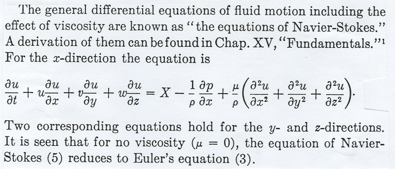
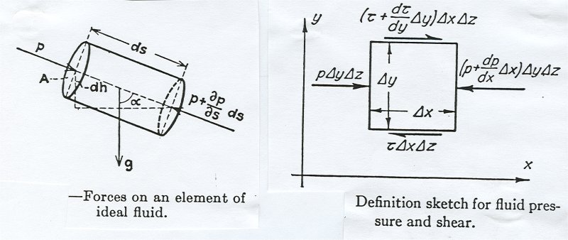
Maxwell's Equations

The numerical solution of Maxwell's Equations for electro-magnetic fields may use a large four dimensional array with dimensions X, Y, Z, T. Three spatial dimensions and time. Relaxation algorithms map well to a four dimensional array of parallel processors. A 4D 12,288 node supercomputer A multiprocessor may have distributed memory, shared memory or a combination of both.
For the distributed memory and the shared memory multiprocessors, one possible connection, shown as a line above, is to use an omega network. The basic building block of an omega network is a switch with two inputs and two outputs. When a message arrives at this switch, the first bit is stripped off and the switch is set to: straight through if the bit is '0' on the top input or '1' on the bottom input else cross connected. Note that only one message can pass, the other being blocked, if two messages arrive and the exclusive or of the first bits is not '1'.
Then omega networks for connecting two devices, four devices or eight devices are built from this switch are shown below. The messages are sent with the most significant bit of the destination first.
For 16 devices connected to the same or different 16 devices, the omega network is built from the primitive switch as:
Note that connecting N devices requires N log_2(N) switches. Given a set of random connections of N devices to N devices with an omega network, this is mathematically a permutation, then statistically 1/2 N connections may be made simultaneously. Then, we can call a CPU-memory pair a node, reduce the drawing of a node to a dot, and show a few connection topologies for multiprocessors
"Ports" is the number of I/O ports the node must have. "Max path" is the maximum number of hops a message must take in order to get from one node to the farthest node. A message may be as small as a Boolean signal or as large as a big matrix. The actual interconnect technology for those lines between the nodes has great variety. The lowest cost is Gigabit Ethernet while the best performance is with Myrinet and Infiniband.
Now, the change 6 years later November 2012 Interconnect Top 500 Count Share (%) Gigabit Ethernet 159 31.8 Infiniband QDR 106 21.2 Infiniband 59 11.8 Custom Interconnect 46 9.2 Infiniband FDR 45 9.0 10G Ethernet 30 6.0 Cray Gemini interconnect 15 3.0 Proprietary 11 2.2 Infiniband DDR 9 1.8 Aries interconnect 4 0.8 Infinband DDR 4x 4 0.8 XT4 Internal Interconnect 4 0.8 Tofu interconnect 3 0.6 Myrinet 10G 3 0.6 Infiniband QDR Sun M9 1 0.2 new 100Gb/sec Ethernet Mellanox 100G One measure of a multiprocessors communication capability is "bisection bandwidth". Optimally choose to split the processors into two equal groups and measure the maximum bandwidth that may be obtained between the groups. Many modern multiprocessors are "clusters." Each node has a CPU, RAM, hard drive and communication hardware. The CPU may be dual or quad core and each CPU is considered a processor that may be assigned tasks. There is no display, keyboard, sound or graphics. The physical form factor is often a "blade" about 2 inches thick, 8 inches high and 12 inches deep with slide in connectors on the back. A blade may have multiple CPU chips each with multiple cores. 40 or more blades may be on one rack. Upon power up, each blade loads its operating system and applications from its local disk. There is still a deficiency in some multiprocessor and multi core operating systems. The OS will move a running program from one CPU to another rather than leave a long running program and its cache contents on one processor. Communication between multiprocesses may actually go out of a communication port and back into a communication processor when the processors are physically connected to the same RAM, rather than use memory to memory communication. Another classification of multiprocessors is: SISD Single Instruction Single Data (e.g. old computer) SIMD Single Instruction Multiple Data (e.g. MASSPAR, CELL, GPU) MIMD Multiple Instruction Multiple Data (e.g. cluster) GPU stands for graphics processing unit, e.g. your graphics card that may have as many as 500 cores. Some of these cards have full IEEE double precision floating point in every core. There may be groups of cores that are SIMD and thus a group may be MIMD. There are three main problems with massively parallel multiprocessors: software, software and software. The operating systems are marginally useful for multiprogramming where a single program is to be run on a single data set using all the nodes and all the memory. Today, the OS is almost no help and the programmer must plan and program each node and every data transfer between nodes. The programming languages are of little help. Java threads and Ada tasks are not guaranteed to run on individual processors. Posix threads are difficult to use and control. MPI and VPM libraries allow the programmer to specifically allocate tasks to nodes and control communication at the expense of significant programming effort. Then there are programming classifications: SPSD Single program Single Data (Conventional program) SPMD Single Program Multiple Data (One program with "if" on all processors) MPMD Multiple Program Multiple Data (Each processor has a unique program) MPI Message Passing Interface is one of the SPMD toolkits that make programming distributed memory multiprocessors practical, yet still not easy. There is a single program that runs on all processors with the allowance for if-then-else code dependent on processor number. The processor number may also be used for index and other calculations. My CMSC 455 lecture on MPI For shared memory parallel programming, threads are used, with one thread typically assigned to each cpu. Only a small percent of application are in the class of "embarrassingly parallel". Most applications require significant design effort to obtain significant "speedup". Yes, Amdahl's law applies to multiprocessors. Given a multiprocessor with N nodes, the maximum speedup to be expected compared to a single processor of the same type as the node, is N. That would imply that 100% of the program could be made parallel. Given 32 processors and 50% of the program can be made fully parallel, 25% of the program can use half the processors and the rest of the program must run sequentially, what is the speedup over one sequential processor? Time sequentially is 100% 100% 50% 25% 25% speedup = ------ = 3.55 Time multiprocessing is --- + --- + --- = 28.125% 28.125% 32 16 1 far from the theoretical maximum of 32! Note: "fully parallel" means the speedup factor is the number of processors. "half the processors" in this case is 32/2 = 16. the remaining 25% is sequential, thus factor = 1 Given 32 processors and 99% of the program can be fully parallel, Time sequentially is 100% 100% 99% 1% speedup = ------ = 24.4 Time multiprocessing is --- + -- = 4.1% 4.1% 32 1 about 3/4 the theoretical maximum of 32! These easy calculations are only considering processing time. In many programs there is significant communication time to get the data to the required node and get the results to the required node. A few programs may require more communication time than computation time. Consider a 1024 = 2^10 node multiprocessor. Add 1,048,576 = 2^20 numbers as fast as possible on this multiprocessor. Assume no communication cost (very unreasonable) step action 1 add 2^10 numbers to 2^10 numbers getting 2^10 partial sums 2 add 2^10 numbers to 2^10 numbers getting 2^10 partial sums ... 2^9=512 add 2^10 numbers to 2^10 numbers getting 2^10 partial sums (so far fully parallel, now have only 2^19 numbers to add) 2^9+1 add 2^10 numbers to 2^10 numbers getting 2^10 partial sums 2^9+2 add 2^10 numbers to 2^10 numbers getting 2^10 partial sums ... 2^9+2^8 add 2^10 numbers to 2^10 numbers getting 2^10 partial sums (so far fully parallel, now have only 2^18 numbers to add) see the progression: 2^9 + 2^8 + 2^7 + ... 2^2 + 2^1 + 2^0 = 1023 time steps and we now have 2^10 partial sums, thus only 2^9 or 512 processors can be used on the next step 1024 add 2^9 numbers to 2^9 numbers getting 2^9 partial sums (using 1/2 the processors) 1025 add 2^8 numbers to 2^8 numbers getting 2^8 partial sums (using 1/4 the processors) ... 1033 add 2^0=1 number to 2^0=1 number to get the final sum (using 1 processor) sequential time 1,048,575 Thus our speedup is --------------- = ----------- = 1015 parallel time 1033 The percent utilization is 1015/1024 * 100% = 99.12% Remember: Every program has a last, single, instruction to execute. Jack Dongarra, an expert in the field of multiprocessor programming says "It just gets worse as you add more processors." Top 500 multiprocessors: These have been and are evaluated by the Linpack Benchmark. Heavy duty numerical computation. This Benchmark is close to "embarrassingly parallel" and thus there is the start of a move to the Graph 500 Benchmark that more fully measures the interconnection capacity of the highly parallel machine. Graph500 Some history of the top500: www.top500.org/lists/2006/06 www.top500.org/list/2007/11/100 www.top500.org/lists/2008/11 www.top500.org/list/2015/06 Over 1 million cores, over 12 megawatts of power. exascale Gemini interconnect trying to solve the biggest problem Latest VA Tech Machine Test your dual core, quad core, 8, 12 to be sure your operating system is assigning threads to different cores. time_mp2.c time_mp4.c time_mp8.c time_mp12.c time_mp12_c.out Here is a graph of Amdahl speedup for increasing number of processors, for 50%, 75%, 90% and 95% parallel execution. As the curves flatten out, more processors or cores are useless.
Project part3a hints diff1.png diff2.png
Covered on web: Previous Final Exam and Answers

Read over course WEB pages. (some have been updated)

Work all homeworks. (some similar problems on exam)

Do project at least through part2b. (some questions on exam)
  Open book, open note, download, edit, submit
  Do not guess, you can look up the answer.
  You may think you know the answer because you saw the
  question before. "no" or "not" may have been added or
  deleted. "some" and "all" are different.
  Numbers and names can change.
  My goal is to make you read carefully so you do
  good on your first employment.

  Edit by placing an  x  after  a)  b)  c)  that is your answer.
  OK to highlight answer.
  Only one answer per question!
  Edit with Microsoft Word on Windows, libreoffice on linux.gl

  Finish homework and projects.

  Students with email user name starting  a b c d e f g h i
  download and edit  final33a.doc
  download final33a.doc


  Students with email user name starting  j k l m n o p q
  download and edit  final33b.doc
  download final33b.doc


  Students with email user name starting  r s t u v w x y z
  download and edit  final33c.doc
  download final33c.doc

  Follow instructions in exam, edit, then
  submit  cs411  final  final32?.doc

  You can do the exam on linux.gl.umbc.edu in your directory

  cp /afs/umbc.edu/users/s/q/squire/pub/download/final33?.doc .
  libreoffice final33?.doc
  submit cs411 final final33?.doc

  rm final33?.doc only if over quota
  Everything due by Dec  12,2020
  Due date changed on a,b,c on Dec 9,2020  same exam.

  Before Exam:
  Review HW2, HW3, HW4 (VHDL) and HW5
  Review WEB Lecture's 14 through 29.

  There are  10  types of people:
    Those who know binary.
    Those who do not know binary.
    Bit numbers start with zero for least significant bit.
    In most languages, the first index is zero.

  Teach your children to count in the computer age:
    zero
    one
    two
    three
    four

  Computer bits are numbered from the bottom

    0  0  1  0  1  = 5
    4  3  2  1  0    bit numbers (actually powers of 2)
last updated Dec 9, 2020
Last updated 10/28/09
