submit midterm and final
 The "submit" facility only works on the "gl" machines.
 The student commands are:
    submit   cs411 HW1 file   puts your "file" into your cs411 HW4
    submitrm cs411 HW1 file   removes your "file" from your cs411 HW4
    submitls cs411 HW1        lists your files in your cs411 HW4

    same for all homeworks, projects, exams
 Once graded, not graded again. Wait until you are finished before submitting.

 Note: For this semester the 'HW1' can be
       HW2, HW3 .... capital H, capital W
       proj1, proj2a, proj2b, proj 3a, proj3b
       mid, fin

       a) you must have your userid registered for "submit"
          send mail from a gl machine to squire if your submit fails
       b) you have to be logged onto a gl machine, putty or ssh are OK
       c) everything is case sensitive, sorry about the uppercase HW.
Do your own homework!
You can discuss homework with other class members but DO NOT COPY!
No "matching answers". No telling others your answers.
All parties involved in copying get zero on that assignment.
Homework 1
Homework 2
Homework 3
Homework 4
Homework 5
Homework 6
Midterm Exam
Other Links
     The answer is just two columns. The first column is the numbers
     1 through 26, the second column is the answer letter.
     Use each letter only once. Find the best fit.
     from the set {a-z}. Match the letter list with the number list.

     1  central processing unit
     2  very large scale integration
     3  another name for a computer
     4  flaw (as in a wafer)
     5  an amplifier (solid state device)
     6  a wafer is cut up into many
     7  a place for instructions and data
     8  digital logic gate
     9  dynamic random access memory
    10  a device made by putting impurities into silicon
    11  high level description of the important information
    12  percent of chips that are good
    13  most significant bit, often the sign bit
    14  memory on the CPU holding recent instructions and data
    15  binary digit
    16  OS
    17  ISA
    18  the basic unit of a computer program
    19  large group of processors used as one computer
    20  the paths where data flows
    21  arithmetic logic unit
    22  circuits that direct the flow in datapaths
    23  converts statements to computer instructions
    24  upward compatible computers
    25  the result of building a design
    26  IC

     a  abstraction        n  VLSI
     b  bit                o  instruction set architecture
     c  MSB                p  DRAM
     d  ALU                q  instruction
     e  CPU                r  operating system
     f  cache              s  supercomputer
     g  control            t  implementation
     h  datapath           u  integrated circuit
     i  compiler           v  transistor
     j  computer family    w  processor
     k  die                x  semiconductor
     l  defect             y  Memory
     m  nand               z  yield

     submit cs411 HW1 your.file
       You do not have to copy the questions, but show the
       computation and clearly indicate the answers.
       Be sure to label the answers with the part number.

 You are the lead designer of a new processor. The processor design
 and compiler are complete, and now you must decide whether to
 produce the current design as it stands or spend additional time
 to improve it. You discuss this problem with your engineering
 team and arrive at the following options:

 a) Leave the design as it stands. Call this the base machine, MBASE.
    It has a clock rate of 1.5GHz and the following measurements have
    been made using a simulator:

   instruction class  CPI  Frequency of use
             A         2     35%
             B         3     20%
             C         4     30%
             D         5     15%

 b) Optimize the hardware. The hardware team claims they can improve
    the processor design to give a clock rate of 3.0GHz.
    The changes cause the CPI of some instructions to change. Call this
    machine MOPT. The compiler team has made changes for this machine.
    The following measurements have been made using a simulator:

   instruction class  CPI  Frequency of use
            A          3     40%
            B          4     30%
            C          4     20%
            D          5     10%

Part1: a) What is the average CPI of MBASE?
       b) What is the average CPI of MOPT?

Part2: a) What is the MIPS rating of MBASE?
       b) What is the MIPS rating of MOPT?

Part3: How much faster is MOPT compared to MBASE?
       "How much faster" is a dimensionless ratio   faster/slower,
       this is called "speed up" always greater than 1.0,
       else "slow down" if less than 1.0

Part4: Using Amdahl's law:
       Suppose we enhance a machine to make all floating point
       instructions run four times faster. Look at how speedup
       behaves when we incorporate faster floating point hardware.
       If the execution time of some benchmark before floating
       point enhancement is 15 seconds total, what is the speedup
       if one-third of the 15 seconds was spent executing
       floating point instructions?

Part5: What is the speedup if three-fourths of the 15 seconds was spent
       executing floating point instructions?

Part6: How many total seconds did Part5 run with the speedup?

Part7: Using Amdahl's law:
       You are going to enhance a machine and there are two possible
       improvements: Either make multiply instructions run four
       times faster than before, or make memory access instructions
       run three times faster than before. A program takes 100 seconds
       to execute before enhancement. 25% of the time is used by
       multiply instructions, 45% of the time is used by memory
       access instructions and the remaining 30% is used by other
       instructions.

  a) What is the speedup from just improving multiply instructions?
  b) What is the speedup from just improving memory access instructions?
  c) What is the speedup from improving both?

     (Use your calculator, exam will have problems like this.)

  submit cs411 HW2 your.file
  Using the program  matmul2.c  from here or  Downloadable source:
  cp /afs/umbc.edu/users/s/q/squire/pub/download/matmul2.c  . # the dot is part of the command

  On a GL Linux machine, linux.gl.umbc.edu only,
  note  fmull  becomes   mulsd  becomes  mulpd   with new versions

  Note: The answers may not be unique. It depends on which
  compiler is used, which specific machine is used and
  which options are used.


  This assignment must be run on linux.gl.umbc.edu machine using:
    gcc -S -O3 matmul2.c
    gcc -g3 -O3 matmul2.c
             ^_____ letter upper case oh,  NOT  zero !

  --------------------------------------------------------------------

        for getting assembly language source code to a file matmul2.s

        gcc -S -O3  matmul2.c       (creates matmul2.s)

  Now, look in the file  matmul2.s

  When running with redirection, ">", first test without redirection
  to be sure you can type the correct input and it works.  Then
  type carefully or use a script to make the redirected run.
  Extra "enter" keys may be needed at various places.

  In  hex.out  use  an address to relate to memory to find the same word.
  Ignore information and error messages. Type very carefully!

  gcc -g3 -O3 matmul2.c  # compile and link, creates file  a.out

  Test first without redirection to hex.out

  gdb a.out
  list 1,26
                  # press enter
  break main
  run
  disassemble
                  # press enter
                  # press enter
  x/60x main
  q
  y

  Now make the file  hex.out  you will turn in as homework:

  gdb a.out > hex.out
  list 1,26
  break main
  run
  disassemble
  x/60x main
  q
  y


  !!!you will see nothing as you are typing, all going into hex.out!!!

  Read the hex dump as big endian, like the MIPS architecture,
  rather than little endian like the X86 architecture, answer
  in 32 bit = 4 byte results, two hex digits per byte.

  The file hex.out has the source listing with line numbers,
  the hex address and hex instructions as loaded in memory and
  the disassembly with hex address and decoded instruction.

  Most of the instruction in the loop are "housekeeping", there are various
  instructions for loading and storing data.


HW3 questions, plus, turn in your hex.out file:

a) How many floating point multiply instructions in matmul2.s ?
b) Do all the instructions have the same names in  matmul2.s  and  hex.out ?
c) Find a  mulpd  instruction in hex.out [use this for c) and d) ]
   Write an assembly language line, write the machine address.
d) From the machine address, look up and write the  mulpd  instruction
   as hexadecimal. Treat as big endian, 32 bit MIPS architecture, rather
   than little endian, X86 architecture.

Attach, or include answers in your "hex.out" file.
(You may edit answers a) b) c) and d) into  front of  hex.out  file or
 send them separately, be sure your name is in all files)

submit cs411 HW3 hex.out
  First:Get yourself set up to use a VHDL compiler/simulator.
        You may use Cadence VHDL or GHDL system.

        To use the Cadence VHDL on linux.gl.umbc.edu.
        Follow instructions exactly or you figure out a variation.
        Be on some computer with ssh, Putty, TeraTerm. Type commands:
        (This will make a sub directory, do not create your own.)

  ssh  your-user-name@linux.gl.umbc.edu #or use Putty or TeraTerm
              (type in your password when asked)

  Right after you log into GL do the following commands:
    mkdir cs411
    cd cs411
    mkdir vhdl2
    cd vhdl2
    cp /afs/umbc.edu/users/s/q/squire/pub/download/cadence_setup.tar .
    tar -xvf cadence_setup.tar
    cp /afs/umbc.edu/users/s/q/squire/pub/download/Makefile_411 .
    cp /afs/umbc.edu/users/s/q/squire/pub/download/Makefile_ghdl .

  You will need to download additional files for each of the
  five projects: part1, part2a, part2b, part3a, part3b.
  You can use cadence simulator or GHDL simulator or both.

  Do all your editing and work in directory  ~/cs411/vhdl2
  This will be used for HW4, HW6, part1, part2, ...
  You may delete the  .tar  file.


        To use GHDL on linux.gl.umbc.edu
        Follow these instructions:

  Now you need more starter files to do HW4:

  cp /afs/umbc.edu/users/s/q/squire/pub/download/add32pg_start.vhdl  .
  cp /afs/umbc.edu/users/s/q/squire/pub/download/tadd32.vhdl  .
  cp /afs/umbc.edu/users/s/q/squire/pub/download/tadd32.run   .
  cp /afs/umbc.edu/users/s/q/squire/pub/download/tadd32.chk   .
  cp /afs/umbc.edu/users/s/q/squire/pub/download/tadd32.chkg   .

  Then  cp  add32pg_start.vhdl  add32.vhdl
  OK to first  mv add32.vhdl add32_pre.vhdl  # to save previous

  Then complete HW4 in add32.vhdl . Fill in for  ...
  You need a 32 bit adder, so use eight instances of add4pg and
  two instances of pg4 in an add32 architecture.

  Connect the circuit per the schematic. The two 16 bit adders
  are connected end to end to make a 32 bit adder.
  cin goes into the first pg4, the carry out from the second
  pg4 gets the signal name  cout.
  Use unique signal names or unique subscripts. All connections with
  the same name are tied together and have the same value.


  After editing add32.vhdl to make it a very fast PG adder:
  make -f Makefile_411 tadd23.out    # runs cadence simulator
  make -f Makefile_ghdl tadd32.gout  # runs GHDL simulator

  Check for errors:
  diff -iw tadd32.out tadd32.chk    # cadence check
  diff -iw tadd32.gout tadd32.chkg  # GHDL check

  Fix  add32.vhdl  for any differences.
  (Ignore any lines with squire, they are from my runs.)

  When checked "submit" a single file named add32.vhdl
  that is a fast PG 32 bit adder.
  Submit  ONE file  add32.vhdl  that has everything in it.

  submit cs411 HW4 add32.vhdl


  You will use the add32.vhdl file in the project, don't trash it.
  It is not important what the signal names are inside add32.vhdl,
  but keep the same interface, the entity declaration.


  Your circuits must run. Incorrect results lose points.

  Debugging: Find the lowest bit that is wrong in the first output
  that does not compare. Proofread the numbers and signal names.
  if 'cout' is a 'U' rather than '0' or '1', there is a break in
  the adder chain. Unfortunately, the hex output converts 'U'
  undefined and 'X' don't know to zero, so you do not see the error.

  Follow the links below to Project and Download for more information.
  See the writeups on VHDL and sample circuits.
  The building blocks may become part of your final project.
After editing add32.vhdl to make it a very fast PG adder:
make -f Makefile_411 tadd23.out # runs cadence simulator
make -f Makefile_ghdl tadd32.gout # runs GHDL simulator
Check for errors:
diff -iw tadd32.out tadd32.chk # cadence check
diff -iw tadd32.gout tadd32.chkg # GHDL check
Fix add32.vhdl for any differences.
(Ignore any lines with squire, they are from my runs.)
When checked "submit" a single file named add32.vhdl
that is a fast PG 32 bit adder.
Submit ONE file add32.vhdl that has everything in it.
submit cs411 HW4 add32.vhdl
You will use the add32.vhdl file in the project, don't trash it.
It is not important what the signal names are inside add32.vhdl,
but keep the same interface, the entity declaration.
Your circuits must run. Incorrect results lose points.
Debugging: Find the lowest bit that is wrong in the first output
that does not compare. Proofread the numbers and signal names.
if 'cout' is a 'U' rather than '0' or '1', there is a break in
the adder chain. Unfortunately, the hex output converts 'U'
undefined and 'X' don't know to zero, so you do not see the error.
Follow the links below to Project and Download for more information.
See the writeups on VHDL and sample circuits.
The building blocks may become part of your final project.
Do not minimize. The grader has only the plain answers.
1. Write two VHDL statements that implement the truth table below
Just use "and" "or" and "not" with parenthesis.
the answer starts x <=
y <=
a b c | x y
------+----
0 0 0 | 0 0
0 0 1 | 0 0
0 1 0 | 1 0
0 1 1 | 1 1
1 0 0 | 0 1
1 0 1 | 0 1
1 1 0 | 1 0
1 1 1 | 0 0
Use this style, do not minimize.
2.Write the VHDL statement that implements the logic diagram, do not simplify
+----+
a --|OR |____
b --| | |
+----+ | +----+
--| XOR|
+----+ | |
c --|AND |_____| |__
d --| | | | |
+----+ | | |
--| | |
+----+ | | | |
e --|NOT |---| +----+ | +----+
+----+ |--| OR |
| |-- g
f ------------------------| |
+----+
Be sure to include the semicolon in VHDL statements,
else you lose one point for each that is missing.
3. Draw the logic diagram that represents the VHDL statement
OK to use gimp or Microsoft.
g <= ((not a and b) xor (c or d or not e)) or (d and not f);
Do not minimize, use class shown logic symbols.
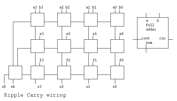
4. For the following schematic, Ripple Carry wiring:
Use a, b, e and f all as four ones. e.g. a <= "1111" etc.
4a) what is the six bit result s.
4b) given that the time from any input to any output in the
full adder is 2T, how much time does the longest path from
any input to any output require? the answer is ____ T
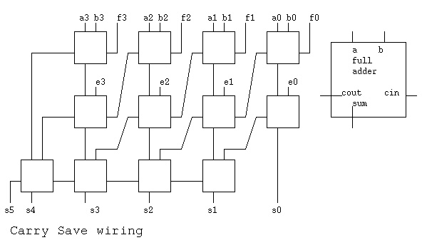
 5. For the following schematic, Carry Save wiring:
Use a, b, e and f all as four ones. e.g. a <= "1111" etc.
5a) what is the six bit result s.
5b) given that the time from any input to any output in the
full adder is 2T, how much time does the longest path from
any input to any output require? the answer is ____ T
5. For the following schematic, Carry Save wiring:
Use a, b, e and f all as four ones. e.g. a <= "1111" etc.
5a) what is the six bit result s.
5b) given that the time from any input to any output in the
full adder is 2T, how much time does the longest path from
any input to any output require? the answer is ____ T
 remember, basic digital logic
submit cs411 HW5 your.file1 your.file2 ...
remember, basic digital logic
submit cs411 HW5 your.file1 your.file2 ...
This homework requires the creation, minimization and use of two small
VHDL entities and the corresponding architectures. The size of the
multiplier depends on your major. This semester, everyone use pmul16.
Design:
Design this homework for an 16 bit by 16 bit parallel multiplier
that produces an unsigned 32 bit product. Submit your design as pmul16.vhdl.
use pmul16_test.vhdl, pmul16_test.run, pmul16_test.chk
By now you know how to get files:
cp /afs/umbc.edu/users/s/q/squire/pub/download/pmul4.vhdl .
cp pmul4.vhdl pmul16.vhdl # please change comments to agree with your code
cp /afs/umbc.edu/users/s/q/squire/pub/download/pmul16_test.vhdl .
cp /afs/umbc.edu/users/s/q/squire/pub/download/pmul16_test.run .
cp /afs/umbc.edu/users/s/q/squire/pub/download/pmul16_test.chk .
cp /afs/umbc.edu/users/s/q/squire/pub/download/pmul16_test.chkg .
Start:
For starting the homework you are given a 4 bit
by 4 bit parallel multiplier that produces an 8 bit unsigned
product. Most of the 4 x 4 code is parametrized using VHDL
generate statements, thus converting to 16 x 16 code
code is supposed to be relatively easy.
Be sure to change all comments also.
The 4 bit by 4 bit multiply to produce a 16 bit unsigned product is
 The component madd circuit is
 The above circuit must be minimized for the top row. Name it madd1
and copy the entity and architecture for madd to madd1 and remove
the first two inputs and statements using these inputs that have
a value '0'.
Start with VHDL source code for pmul4 (shown below)
Change pmul4 to pmul16 for use in project part1
N:=3 to N:=15
3 downto 0 to 15 downto 0
7 downto 0 to 31 downto 0
Compile and run, check output before creating two new entities.
diff -iw pmul16_test.out pmul16_test.chk
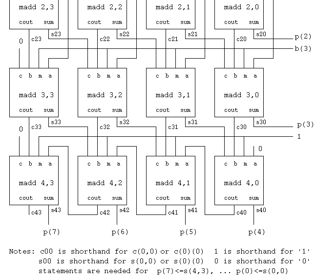
pmul4.vhdl parallel multiply 4 bit x 4 bit to get 16 bit unsigned product
uses VHDL 'generate' to have less statements
see diagram madd.jpg for madd schematic
see diagram pmul4.ps for pmul4 schematic
library IEEE;
use IEEE.std_logic_1164.all;
entity madd is -- multiplying full adder stage
port(c : in std_logic; -- one input, think carry in
b : in std_logic; -- one input, think previous sum
m : in std_logic; -- multiplier bit
a : in std_logic; -- multiplicand bit
sum : out std_logic; -- carry save sum out
cout : out std_logic); -- carry save carry out
end entity madd;
architecture circuits of madd is -- multiplying full adder stage
signal aa: std_logic;
begin
aa <= a and m; -- logic could be reduced, yet probably circuit designed
sum <= (aa and b and c) or (aa and not b and not c) or
(not aa and b and not c) or (not aa and not b and c) after 1 ns;
cout <= (aa and b) or (aa and c) or (b and c) after 1 ns;
end architecture circuits; -- of madd
library IEEE;
use IEEE.std_logic_1164.all;
entity pmul4 is -- 4 x 4 = 8 bit unsigned product multiplier
port(a : in std_logic_vector(3 downto 0); -- multiplicand
b : in std_logic_vector(3 downto 0); -- multiplier
p : out std_logic_vector(7 downto 0)); -- product
end pmul4;
architecture circuits of pmul4 is
constant N : integer := 3; -- last row number
constant NP : integer := N+1; -- last row plus 1
constant NM : integer := N-1; -- last row minus 1
type arr is array(0 to NP) of std_logic_vector(N downto 0);
signal s : arr; -- partial sums
signal c : arr; -- partial carries
signal zero : std_logic := '0';
begin -- circuits of pmul4
-- the internal part of the multiplier is nested generate
-- special case generate is needed for the top row,
-- the bottom row, the left column and
-- connecting to the product outputs.
-- center
gmaddi: for i in 1 to N generate
gmaddj: for j in 0 to NM generate
maddij: entity WORK.madd
port map(s(i-1)(j+1), c(i-1)(j), b(i), a(j), s(i)(j), c(i)(j));
end generate gmaddj;
end generate gmaddi;
-- top row replace WORK.madd with your WORK.madd1, remove zero's
gmadd0j: for j in 0 to N generate
madd0j: entity WORK.madd
port map(zero, zero, b(0), a(j), s(0)(j), c(0)(j));
end generate gmadd0j;
-- left column
gmaddiN: for i in 1 to N generate
maddiN: entity WORK.madd
port map(zero, c(i-1)(N), b(i), a(N), s(i)(N), c(i)(N));
end generate gmaddiN;
-- bottom row
maddNP0: entity WORK.madd
port map(s(N)(1), c(N)(0), '1', '0', s(NP)(0), c(NP)(0));
maddNPN: entity WORK.madd
port map(zero, c(N)(N), '1', c(NP)(NM), s(NP)(N), c(NP)(N));
gmaddNP: for j in 1 to NM generate
maddNPj: entity WORK.madd
port map(s(N)(j+1), c(N)(j), '1', c(NP)(j-1), s(NP)(j), c(NP)(j));
end generate gmaddNP;
-- connect outputs
gp0i: for i in 0 to N generate
p0i: p(i) <= s(i)(0);
pNi: p(i+NP) <= s(NP)(i);
end generate gp0i;
end architecture circuits; -- of pmul4
Notice that the only component used to build the multiplier
is "madd" and some uses of "madd" have constants as inputs.
Copy pmul4.vhdl to pmul16.vhdl
Edit pmul16.vhdl and replace all "pmul4" with "pmul16"
Look through the VHDL and change inputs from
(3 downto 0) to (15 downto 0).
Note: 4 bit numbers are (3 downto 0) in VHDL,
and 16 bit numbers are (15 downto 0) in VHDL. Thus, the
constant N goes from 3 to 15 when going from 4 bits to 16 bits.
See Lecture 12 to simplify
Look at the difference between samples.html sqrt8 and sqrt8m
Notice how the "Sm" component was simplified for "S0" and "S1".
This is the idea for your simplifying "madd".
For testing your pmul16 component download pmul16_test.vhdl and pmul16_test.run
and pmul16_test.chk
cp /afs/umbc.edu/users/s/q/squire/pub/download/pmul4.vhdl .
cp /afs/umbc.edu/users/s/q/squire/pub/download/pmul16_test.vhdl .
cp /afs/umbc.edu/users/s/q/squire/pub/download/pmul16_test.run .
cp /afs/umbc.edu/users/s/q/squire/pub/download/pmul16_test.chk .
cp /afs/umbc.edu/users/s/q/squire/pub/download/pmul16_test.chkg . #for GHDL
cp pmul4.vhdl pmul16.vhdl # make changes per above
For cadence use Makefile_411, now make
make -f Makefile_411 pmul16_test.out
or type
For GHDL use Makefile_ghdl, now make
make -f Makefile_ghdl pmul16_test.gout
or type
ghdl -a --ieee=synopsys pmul16.vhdl
ghdl -a --ieee=synopsys pmul16_test.vhdl
ghdl -e --ieee=synopsys pmul16_test
ghdl -r --ieee=synopsys pmul16_test --stop-time=8704ns > pmul16_test.out
Now run the simulation by typing make
Then check by typing
diff -iw pmul16_test.out pmul16_test.chk
diff -iw pmul16_test.out pmul16_test.chkg # for GHDL
Everything is correct if there are no differences other than
the copyright line.
submit cs411 HW6 pmul16.vhdl
The above circuit must be minimized for the top row. Name it madd1
and copy the entity and architecture for madd to madd1 and remove
the first two inputs and statements using these inputs that have
a value '0'.
Start with VHDL source code for pmul4 (shown below)
Change pmul4 to pmul16 for use in project part1
N:=3 to N:=15
3 downto 0 to 15 downto 0
7 downto 0 to 31 downto 0
Compile and run, check output before creating two new entities.
diff -iw pmul16_test.out pmul16_test.chk
pmul4.vhdl parallel multiply 4 bit x 4 bit to get 16 bit unsigned product
uses VHDL 'generate' to have less statements
see diagram madd.jpg for madd schematic
see diagram pmul4.ps for pmul4 schematic
library IEEE;
use IEEE.std_logic_1164.all;
entity madd is -- multiplying full adder stage
port(c : in std_logic; -- one input, think carry in
b : in std_logic; -- one input, think previous sum
m : in std_logic; -- multiplier bit
a : in std_logic; -- multiplicand bit
sum : out std_logic; -- carry save sum out
cout : out std_logic); -- carry save carry out
end entity madd;
architecture circuits of madd is -- multiplying full adder stage
signal aa: std_logic;
begin
aa <= a and m; -- logic could be reduced, yet probably circuit designed
sum <= (aa and b and c) or (aa and not b and not c) or
(not aa and b and not c) or (not aa and not b and c) after 1 ns;
cout <= (aa and b) or (aa and c) or (b and c) after 1 ns;
end architecture circuits; -- of madd
library IEEE;
use IEEE.std_logic_1164.all;
entity pmul4 is -- 4 x 4 = 8 bit unsigned product multiplier
port(a : in std_logic_vector(3 downto 0); -- multiplicand
b : in std_logic_vector(3 downto 0); -- multiplier
p : out std_logic_vector(7 downto 0)); -- product
end pmul4;
architecture circuits of pmul4 is
constant N : integer := 3; -- last row number
constant NP : integer := N+1; -- last row plus 1
constant NM : integer := N-1; -- last row minus 1
type arr is array(0 to NP) of std_logic_vector(N downto 0);
signal s : arr; -- partial sums
signal c : arr; -- partial carries
signal zero : std_logic := '0';
begin -- circuits of pmul4
-- the internal part of the multiplier is nested generate
-- special case generate is needed for the top row,
-- the bottom row, the left column and
-- connecting to the product outputs.
-- center
gmaddi: for i in 1 to N generate
gmaddj: for j in 0 to NM generate
maddij: entity WORK.madd
port map(s(i-1)(j+1), c(i-1)(j), b(i), a(j), s(i)(j), c(i)(j));
end generate gmaddj;
end generate gmaddi;
-- top row replace WORK.madd with your WORK.madd1, remove zero's
gmadd0j: for j in 0 to N generate
madd0j: entity WORK.madd
port map(zero, zero, b(0), a(j), s(0)(j), c(0)(j));
end generate gmadd0j;
-- left column
gmaddiN: for i in 1 to N generate
maddiN: entity WORK.madd
port map(zero, c(i-1)(N), b(i), a(N), s(i)(N), c(i)(N));
end generate gmaddiN;
-- bottom row
maddNP0: entity WORK.madd
port map(s(N)(1), c(N)(0), '1', '0', s(NP)(0), c(NP)(0));
maddNPN: entity WORK.madd
port map(zero, c(N)(N), '1', c(NP)(NM), s(NP)(N), c(NP)(N));
gmaddNP: for j in 1 to NM generate
maddNPj: entity WORK.madd
port map(s(N)(j+1), c(N)(j), '1', c(NP)(j-1), s(NP)(j), c(NP)(j));
end generate gmaddNP;
-- connect outputs
gp0i: for i in 0 to N generate
p0i: p(i) <= s(i)(0);
pNi: p(i+NP) <= s(NP)(i);
end generate gp0i;
end architecture circuits; -- of pmul4
Notice that the only component used to build the multiplier
is "madd" and some uses of "madd" have constants as inputs.
Copy pmul4.vhdl to pmul16.vhdl
Edit pmul16.vhdl and replace all "pmul4" with "pmul16"
Look through the VHDL and change inputs from
(3 downto 0) to (15 downto 0).
Note: 4 bit numbers are (3 downto 0) in VHDL,
and 16 bit numbers are (15 downto 0) in VHDL. Thus, the
constant N goes from 3 to 15 when going from 4 bits to 16 bits.
See Lecture 12 to simplify
Look at the difference between samples.html sqrt8 and sqrt8m
Notice how the "Sm" component was simplified for "S0" and "S1".
This is the idea for your simplifying "madd".
For testing your pmul16 component download pmul16_test.vhdl and pmul16_test.run
and pmul16_test.chk
cp /afs/umbc.edu/users/s/q/squire/pub/download/pmul4.vhdl .
cp /afs/umbc.edu/users/s/q/squire/pub/download/pmul16_test.vhdl .
cp /afs/umbc.edu/users/s/q/squire/pub/download/pmul16_test.run .
cp /afs/umbc.edu/users/s/q/squire/pub/download/pmul16_test.chk .
cp /afs/umbc.edu/users/s/q/squire/pub/download/pmul16_test.chkg . #for GHDL
cp pmul4.vhdl pmul16.vhdl # make changes per above
For cadence use Makefile_411, now make
make -f Makefile_411 pmul16_test.out
or type
For GHDL use Makefile_ghdl, now make
make -f Makefile_ghdl pmul16_test.gout
or type
ghdl -a --ieee=synopsys pmul16.vhdl
ghdl -a --ieee=synopsys pmul16_test.vhdl
ghdl -e --ieee=synopsys pmul16_test
ghdl -r --ieee=synopsys pmul16_test --stop-time=8704ns > pmul16_test.out
Now run the simulation by typing make
Then check by typing
diff -iw pmul16_test.out pmul16_test.chk
diff -iw pmul16_test.out pmul16_test.chkg # for GHDL
Everything is correct if there are no differences other than
the copyright line.
submit cs411 HW6 pmul16.vhdl
  Open book. Multiple choice questions based on reading assignments,
  lectures, web pages, handouts and homework. OK to check back on
  web pages. Do not discus with other students.


  (reading assignments were all covered in lectures, see web pages)

  just instructions  on web
      (nop, j, beq, add, sub, mul, and, or, addi,
       sll, srl, cmpl, lw, sw)

  Exam covers homework: HW1-HW5
  Be sure to go over web pages,
  no questions on current events web pages

  submit cs411 mid mid?.doc
Last updated 9/16/2020 more changes possible